
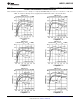
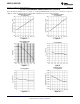
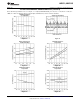
Datasheet
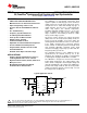
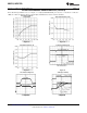
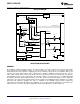

PVIN
SW
AGND
FB
PGOOD
EN
SS/TRK
AVIN
COMP
LM20133
L
R
F
VCC
PGND
C
IN
R
C1
C
C1
V
IN
C
SS
C
VCC
C
OUT
V
OUT
R
FB2
R
FB1
C
F
(optional)
SYNC
LM20133, LM20133Q
www.ti.com
SNVS526F –OCTOBER 2007–REVISED MARCH 2013
3A, PowerWise
®
Synchronous Buck Regulator with Input Synchronization
Check for Samples: LM20133, LM20133Q
1
FEATURES
DESCRIPTION
The LM20133 is a full featured synchronous buck
2
• LM20133Q is AEC-Q100 Qualified and
regulator capable of delivering up to 3A of continuous
Manufactured on an Automotive Grade Flow
output current. The current mode control loop can be
• Input Voltage Range 2.95V to 5.5V
compensated to be stable with virtually any type of
• Accurate Current Limit Minimizes Inductor
output capacitor. For most cases, compensating the
device only requires two external components,
Size
providing maximum flexibility and ease of use. The
• 97% Peak Efficiency
device is optimized to work over the input voltage
• Frequency Synchronization Pin
range of 2.95V to 5.5V making it suited for a wide
• 32 mΩ Integrated FET Switches
variety of low voltage systems.
• Starts up into Pre-Biased Loads
The device features internal over voltage protection
(OVP) and over current protection (OCP) circuits for
• Output Voltage Tracking
increased system reliability. A precision enable pin
• Peak Current Mode Control
and integrated UVLO allows the turn on of the device
• Adjustable Soft-Start with External Capacitor
to be tightly controlled and sequenced. Start-up
• Precision Enable Pin with Hysteresis
inrush currents are limited by both an internally fixed
and externally adjustable Soft-Start circuit. Fault
• Integrated OVP, UVLO, Power Good and
detection and supply sequencing is possible with the
Thermal Shutdown
integrated power good circuit.
• HTSSOP 16-Pin Exposed Pad Package
The switching frequency of the LM20133 can be
synchronized to an external clock by use of the
APPLICATIONS
SYNC pin. The SYNC pin is capable of synchronizing
• Simple to Design, High Efficiency Point of
to input signals ranging from 500 kHz to 1.5 MHz.
Load Regulation from a 5V or 3.3V bus
The LM20133 is designed to work well in multi-rail
• High Performance DSPs, FPGAs, ASICs and
power supply architectures. The output voltage of the
Microprocessors
device can be configured to track a higher voltage rail
using the SS/TRK pin. If the output of the LM20133 is
• Broadband, Networking and Optical
pre-biased at startup it will not sink current to pull the
Communications Infrastructure
output low until the internal soft-start ramp exceeds
the voltage at the feedback pin.
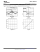
Typical Application Circuit
1
Please be aware that an important notice concerning availability, standard warranty, and use in critical applications of
Texas Instruments semiconductor products and disclaimers thereto appears at the end of this data sheet.
2All trademarks are the property of their respective owners.
PRODUCTION DATA information is current as of publication date.
Copyright © 2007–2013, Texas Instruments Incorporated
Products conform to specifications per the terms of the Texas
Instruments standard warranty. Production processing does not
necessarily include testing of all parameters.