
Datasheet
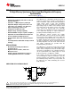
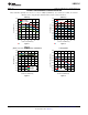

FB
PGOOD
V
IN
LM21212-1
V
OUT
AGND
COMP
PVIN
SYNC
SW
EN
C
IN
C
OUT
L
OUT
R
C1
C
C1
C
C2
C
C3
R
FB1
R
FB2
R
C2
PGND
AVIN
C
F
1
11-16
3
4
17
19
18
20
8,9,10
5,6,7
R
F
SS/
TRK
C
SS
2
optional
HTSSOP-20
optional
LM21212-1
www.ti.com
SNVS671E –FEBRUARY 2011–REVISED MARCH 2013
12A High Efficiency Synchronous Point of Load Buck Regulator with Frequency
Synchronization
Check for Samples: LM21212-1
1
FEATURES
DESCRIPTION
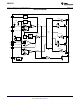
The LM21212-1 is a monolithic synchronous point of
2
• Integrated 7.0 mΩ High Side and 4.3 mΩ Low
load buck regulator that is capable of delivering up to
Side FET Switches
12A of continuous output current while producing an
• 300 kHz to 1.5 MHz Frequency SYNC pin
output voltage down to 0.6V with outstanding
• Adjustable Output Voltage From 0.6V to V
IN
efficiency. The device is optimized to work over an
input voltage range of 2.95V to 5.5V, making it suited
(100% duty cycle capable), ±1% Reference
for a wide variety of low voltage systems. The voltage
• Input Voltage Range 2.95V to 5.5V
mode control loop provides high noise immunity,
• Startup Into Pre-Biased Loads
narrow duty cycle capability and can be compensated
• Output Voltage Tracking Capability
to be stable with any type of output capacitance,
providing maximum flexibility and ease of use.
• Wide Bandwidth Voltage Loop Error Amplifier
The LM21212-1 features internal over voltage
• Adjustable Soft-Start With External Capacitor
protection (OVP) and over-current protection (OCP)
• Precision Enable Pin With Hysteresis
for increased system reliability. A precision enable pin
• Integrated OVP, OCP, OTP, UVLO and Power-
and integrated UVLO allow turn-on of the device to
Good
be tightly controlled and sequenced. Startup inrush
currents are limited by both an internally fixed and
• Thermally Enhanced HTSSOP-20 Exposed Pad
externally adjustable soft-start circuit. Fault detection
Package
and supply sequencing are possible with the
integrated power good circuit.
APPLICATIONS
The LM21212-1 is designed to work well in multi-rail
• Broadband, Networking and Wireless
power supply architectures. The output voltage of the
Communications
device can be configured to track an external voltage
• High-Performance FPGAs, ASICs and
rail using the SS/TRK pin. The switching frequency
Microprocessors
can be synchronized to the falling edge of a clock
between frequencies of 300kHz to 1.5MHz.
• Simple to Design, High Efficiency Point of
Load Regulation From a 5V or 3.3V Bus
If the output is pre-biased at startup, it will not sink
current, allowing the output to smoothly rise past the
pre-biased voltage. The regulator is offered in a 20-
pin HTSSOP package with an exposed pad that can
be soldered to the PCB, eliminating the need for
bulky heatsinks.
SIMPLIFIED APPLICATION CIRCUIT
1
Please be aware that an important notice concerning availability, standard warranty, and use in critical applications of
Texas Instruments semiconductor products and disclaimers thereto appears at the end of this data sheet.
2All trademarks are the property of their respective owners.
PRODUCTION DATA information is current as of publication date.
Copyright © 2011–2013, Texas Instruments Incorporated
Products conform to specifications per the terms of the Texas
Instruments standard warranty. Production processing does not
necessarily include testing of all parameters.