
Datasheet

1
2
3
4
5
10
9
8
7
6
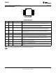
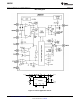
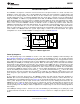
UVLO/EN
FB
PWR
GND
TIMER
PGD
OUTVIN
SENSE
GATE
LM25061
SNVS611E –FEBRUARY 2011–REVISED MARCH 2013
www.ti.com
Connection Diagram
Figure 2. Top View
10-Lead VSSOP
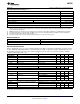
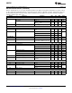
PIN DESCRIPTIONS
Pin # Name Description Applications Information
1 SENSE Current sense input The voltage across the current sense resistor (R
S
) is measured from VIN to this pin. If
the voltage across R
S
reaches 50mV the load current is limited and the fault timer
activates.
2 VIN Positive supply input A small ceramic bypass capacitor close to this pin is recommended to suppress
transients which occur when the load current is switched off.
3 UVLO/EN Under-voltage lockout An external resistor divider from the system input voltage sets the under-voltage turn-
on threshold. An internal 20 µA current source provides hysteresis. The enable
threshold at the pin is 1.17V. This pin can also be used for remote shutdown control.
4 FB Output feedback An external resistor divider from the output sets the output voltage at which the PGD
pin switches. The threshold at the pin is 1.17V. An internal 22 µA current source
provides hysteresis.
5 GND Circuit ground
6 TIMER Timing capacitor An external capacitor connected to this pin sets the insertion time delay and the Fault
Timeout Period. The capacitor also sets the restart timing of the LM25061-2.
7 PWR Power limit set An external resistor connected to this pin, in conjunction with the current sense resistor
(R
S
), sets the maximum power dissipation allowed in the external series pass
MOSFET.
8 PGD Power Good indicator An open drain output. This output is high when the voltages at the FB pin and at the
UVLO pin are above their thresholds.
9 OUT Output feedback Connect to the output rail (external MOSFET source). Internally used to determine the
MOSFET V
DS
voltage for power limiting.
10 GATE Gate drive output Connect to the external MOSFET’s gate. This pin's voltage is limited at 19.5V above
ground.
These devices have limited built-in ESD protection. The leads should be shorted together or the device placed in conductive foam
during storage or handling to prevent electrostatic damage to the MOS gates.
2 Submit Documentation Feedback Copyright © 2011–2013, Texas Instruments Incorporated
Product Folder Links: LM25061