LM25066I, LM25066IA www.ti.com SNVS824C – JUNE 2012 – REVISED MARCH 2013 Intel Node Manager Compliant System Power Management and Protection IC with PMBus Check for Samples: LM25066I, LM25066IA FEATURES DESCRIPTION • While the LM25066I/A is functionally similar to the LM25066/A, the LM25066I/A is fully compliant to Intel Node Manager 2.0, 2.5 and adds the READ_EIN energy accumulator feature. The LM25066I/A combines a high-performance hot-swap controller with a PMBus 1.
LM25066I, LM25066IA SNVS824C – JUNE 2012 – REVISED MARCH 2013 www.ti.com Typical Application Schematic Q2 VIN CIN VOUT RS Q1 DZ R1 VIN CLOAD GATE SENSE OUT R4 DIODE UVLO/EN UVLO/EN R2 FB VDD R5 OVLO R3 RPG VDD ADR2 N/C ADR1 N/C ADR0 PGD LM25066I/A VAUX RETRY SMBA SMBus Interface Auxillary ADC Input (0V - 1.
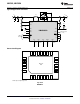
LM25066I, LM25066IA www.ti.com SNVS824C – JUNE 2012 – REVISED MARCH 2013 Pin Descriptions Pin No. Name Description Applications Information Pad Exposed Pad Exposed pad of WQFN package No internal electrical connection. Solder to the ground plane to reduce thermal resistance. 1 ADR2 SMBUS address line 2 3 - state address line. Should be connected to GND, VDD, or left floating. 2 ADR1 SMBUS address line 1 3 - state address line. Should be connected to GND, VDD, or left floating.
LM25066I, LM25066IA SNVS824C – JUNE 2012 – REVISED MARCH 2013 www.ti.com Absolute Maximum Ratings (1) VIN, SENSE to GND (2) -0.3V to 24V GATE, FB, UVLO/EN, OVLO, PGD to GND (2) -0.3V to 20V Out to GND -1 to 20V SCL, SDA, SMBA, CL, CB, ADR0, ADR1, ADR2, VDD, VAUX, DIODE, RETRY to GND -0.3V to 6V VIN to SENSE -0.3V to +0.
LM25066I, LM25066IA www.ti.com SNVS824C – JUNE 2012 – REVISED MARCH 2013 Electrical Characteristics (continued) Limits in standard type are for TJ = 25°C only; limits in boldface type apply over the junction temperature (TJ) range of -40°C to +85°C unless otherwise stated. Minimum and Maximum limits are specified through test, design, or statistical correlation. Typical values represent the most likely parametric norm at TJ = 25°C, and are provided for reference purposes only.
LM25066I, LM25066IA SNVS824C – JUNE 2012 – REVISED MARCH 2013 www.ti.com Electrical Characteristics (continued) Limits in standard type are for TJ = 25°C only; limits in boldface type apply over the junction temperature (TJ) range of -40°C to +85°C unless otherwise stated. Minimum and Maximum limits are specified through test, design, or statistical correlation. Typical values represent the most likely parametric norm at TJ = 25°C, and are provided for reference purposes only.
LM25066I, LM25066IA www.ti.com SNVS824C – JUNE 2012 – REVISED MARCH 2013 Electrical Characteristics (continued) Limits in standard type are for TJ = 25°C only; limits in boldface type apply over the junction temperature (TJ) range of -40°C to +85°C unless otherwise stated. Minimum and Maximum limits are specified through test, design, or statistical correlation. Typical values represent the most likely parametric norm at TJ = 25°C, and are provided for reference purposes only.
LM25066I, LM25066IA SNVS824C – JUNE 2012 – REVISED MARCH 2013 www.ti.com Typical Performance Characteristics Unless otherwise specified the following conditions apply: TJ = 25°C, VIN = 12V. All graphs show junction temperature. VIN Pin Current 5.5 SENSE Pin Current (Enabled) VIN = 17V 5.0 VIN = 12V 4.5 4.0 VIN = 3V 3.5 3.0 -40 -20 0 20 40 60 80 100 120 140 54 SENSE PIN CURRENT (ENABLED) ( A) VIN INPUT CURRENT (mA) 6.0 50 VIN = 17V 46 VIN = 12V 42 38 VIN = 2.
LM25066I, LM25066IA www.ti.com SNVS824C – JUNE 2012 – REVISED MARCH 2013 Typical Performance Characteristics (continued) Unless otherwise specified the following conditions apply: TJ = 25°C, VIN = 12V. All graphs show junction temperature. GATE Pin Source Current Power Limit Threshold 24 POWER LIMIT THRESHOLD (mV) GATE PIN SOURCE CURRENT ( A) 23 22 21 20 VIN = 5V TO 17V 19 18 17 VIN = 2.9V 16 15 20 RPWR 16 12 14 8 RPWR 4 0 20 40 60 80 100 120 140 TEMPERATURE (°C) -40 -20 Figure 7.
LM25066I, LM25066IA SNVS824C – JUNE 2012 – REVISED MARCH 2013 www.ti.com Typical Performance Characteristics (continued) Unless otherwise specified the following conditions apply: TJ = 25°C, VIN = 12V. All graphs show junction temperature. OVLO Threshold OVLO Hysteresis -16 OVLO HYSTERESIS CURRENT ( A) 1.167 OVLO THRESHOLD (V) VIN = 2.9V 1.166 VIN = 12V 1.165 1.164 1.163 VIN = 17V 1.
LM25066I, LM25066IA www.ti.com SNVS824C – JUNE 2012 – REVISED MARCH 2013 Typical Performance Characteristics (continued) Unless otherwise specified the following conditions apply: TJ = 25°C, VIN = 12V. All graphs show junction temperature. Reference Voltage Startup (Insertion Delay) 2.75 INSERTION DELAY = 140 ms VREF (V) 2.74 2.73 2.72 TIMER 1V/DIV VIN 10V/DIV 10V/DIV GATE 2.71 VOUT 10V/DIV 2.70 100 ms/DIV -60 -40 -20 0 20 40 60 80 100120140 TEMPERATURE (°C) Figure 19. Figure 20.
LM25066I, LM25066IA SNVS824C – JUNE 2012 – REVISED MARCH 2013 www.ti.com Typical Performance Characteristics (continued) Unless otherwise specified the following conditions apply: TJ = 25°C, VIN = 12V. All graphs show junction temperature. Current Limit Event (CL = GND) Circuit Breaker Event (CL = CB = GND) 1V/DIV TIMER TIMER TIMEOUT PERIOD = 8.
LM25066I, LM25066IA www.ti.com SNVS824C – JUNE 2012 – REVISED MARCH 2013 24 A LM25066I/A VDD REG VDD REF GEN 1.167V UV OV S/H AMUX 1/16 ID 25 mV VAUX 1M SCL SMBUS INTERFACE VDS 10 A Diode Temp Sense Gate Control 2 mA 190 mA Power Limit Threshold GATE 18.8V Current Limit/ Power Limit Control 5.5 A Insertion Timer SnapShot MEASUREMENT/ AVERAGING FAULT REGISTERS SDA 22 A Current Limit Threshold Gain = 2.
LM25066I, LM25066IA SNVS824C – JUNE 2012 – REVISED MARCH 2013 www.ti.com FUNCTIONAL DESCRIPTION The inline protection functionality of the LM25066I/A is designed to control the in-rush current to the load upon insertion of a circuit card into a live backplane or other “hot” power source, thereby limiting the voltage sag on the backplane’s supply voltage and the dV/dt of the voltage applied to the load. Effects on other circuits in the system are minimized, preventing possible unintended resets.
LM25066I, LM25066IA www.ti.com SNVS824C – JUNE 2012 – REVISED MARCH 2013 voltage reaches 1.7V. CT is then quickly discharged by an internal 1.9 mA pulldown current. The GATE pin then switches on Q1 when VSYS, the input supply voltage, exceeds the UVLO threshold. If VSYS is above the UVLO threshold at the end of the insertion time, Q1 switches on at that time. The GATE pin charge pump sources 22 µA to charge the gate capacitance of Q1.
LM25066I, LM25066IA SNVS824C – JUNE 2012 – REVISED MARCH 2013 www.ti.com Gate Control A charge pump provides the voltage at the GATE pin to enhance the N-Channel MOSFET’s gate. During normal operating conditions (t3 in )Figure 32) the gate of Q1 is held charged by an internal 22 µA current source. The voltage at the GATE pin (with respect to ground) is limited by an internal 18.8 V zener diode. See the graph “GATE Pin Voltage” shown previously.
LM25066I, LM25066IA www.ti.com SNVS824C – JUNE 2012 – REVISED MARCH 2013 active as described in Fault Timer and Restart.
LM25066I, LM25066IA SNVS824C – JUNE 2012 – REVISED MARCH 2013 www.ti.com Under-Voltage Lockout (UVLO) The series pass MOSFET (Q1) is enabled when the input supply voltage (VSYS) is within the operating range defined by the programmable under-voltage lockout (UVLO) and over-voltage lockout (OVLO) levels. Typically the UVLO level at VSYS is set with a resistor divider (R1-R3) as shown in Figure 35.
LM25066I, LM25066IA www.ti.com SNVS824C – JUNE 2012 – REVISED MARCH 2013 voltage at the FB pin is below its threshold, the 24 µA current source at FB is disabled. As the output voltage increases, taking FB above its threshold, the current source is enabled, sourcing current out of the pin, raising the voltage at FB to provide threshold hysteresis. The PGD output is forced low when either the UVLO/EN pin is below its threshold or the OVLO pin is above its threshold.
LM25066I, LM25066IA SNVS824C – JUNE 2012 – REVISED MARCH 2013 www.ti.com The SMBus address of the LM25066I/A is captured based on the states of the ADR0, ADR1, and ADR2 pins (GND, NC, VDD) during turn-on and is latched into a volatile register once VDD has exceeded its POR threshold of 2.6V. Reassigning or postponing the address capture is accomplished by holding the VREF pin to ground. Pulling the VREF pin low will also reset the logic and erase the volatile memory of the LM25066I/A.
LM25066I, LM25066IA www.ti.com SNVS824C – JUNE 2012 – REVISED MARCH 2013 APPLICATIONS SECTION MMBT3904 12V SMCJ15A 0.5 m: VOUT PSMN1R2-25YL 330 PF 25 k: 10 k: VIN SENSE GATE UVLO/EN UVLO/EN 2.1 k: OUT OUT DIODE FB 1.3 k: OVLO 2.1 k: 10 k: VDD ADR2 N/C ADR1 N/C ADR0 PGD LM25066I/IA VAUX Auxillary ADC Input (0V - 1.16V) RETRY SMBA SMBus Interface VDD CB SDA CL SCL VDD VREF 1 PF 1 PF GND TIMER PWR 0.47 PF 6.98 k: Figure 36.
LM25066I, LM25066IA SNVS824C – JUNE 2012 – REVISED MARCH 2013 • • • • • • www.ti.com The BVDSS rating should be greater than the maximum system voltage (VSYS), plus ringing and transients which can occur at VSYS when the circuit card, or adjacent cards, are inserted or removed. The maximum continuous current rating should be based on the current limit threshold (e.g. 25 mV/RS), not the maximum load current, since the circuit can operate near the current limit threshold continuously.
LM25066I, LM25066IA www.ti.com SNVS824C – JUNE 2012 – REVISED MARCH 2013 POWER LIMIT THRESHOLD The LM25066I/A determines the power dissipation in the external MOSFET (Q1) by monitoring the drain current (the current in RS), and the VDS of Q1 (SENSE to OUT pins). The resistor at the PWR pin (RPWR) sets the maximum power dissipation for Q1 and is calculated from Equation 2: RPWR = 1.
LM25066I, LM25066IA SNVS824C – JUNE 2012 – REVISED MARCH 2013 www.ti.com RS Q1 VSYS OUT SENSE VIN PGD LM25066I/A RL CL GND GND Figure 38. A. No Load Current During Turn-On RS Q1 VSYS SENSE VIN OUT CL PGD RL LM25066I/A GND GND Load Draws Current During Turn-On Figure 39. Current During Turn-On B) Turn-On with Power Limit and Current Limit: The maximum allowed power dissipation in Q1 (PMOSFET(LIM)) is defined by the resistor at the PWR pin, and the current sense resistor RS.
LM25066I, LM25066IA www.ti.com SNVS824C – JUNE 2012 – REVISED MARCH 2013 A) Insertion Delay -Upon applying the system voltage (VSYS) to the circuit, the external MOSFET (Q1) is held off during the insertion time (t1 in Figure 32) to allow ringing and transients at VSYS to settle. Since each backplane’s response to a circuit card plug-in is unique, the worst case settling time must be determined for each application.
LM25066I, LM25066IA SNVS824C – JUNE 2012 – REVISED MARCH 2013 www.ti.com VSYS VIN 23 PA R1 UVLO/EN 1.16V R2 1.16V TIMER AND GATE LOGIC CONTROL OVLO R3 23 PA GND LM25066I/A Figure 41. UVLO and OVLO Thresholds Set By R1-R3 The procedure to calculate the resistor values is as follows: • Choose the upper UVLO threshold (VUVH), and the lower UVLO threshold (VUVL). • Choose the upper OVLO threshold (VOVH).
LM25066I, LM25066IA www.ti.com SNVS824C – JUNE 2012 – REVISED MARCH 2013 Option B: If all four thresholds must be accurately defined, the configuration in Figure 42 can be used. VSYS VIN 23 PA R1 UVLO/EN 1.16V TIMER AND GATE LOGIC CONTROL R2 R3 OVLO 1.16V R4 GND 23 PA LM25066I/A Figure 42. Programming the Four Thresholds The four resistor values are calculated as follows: - Choose the upper and lower UVLO thresholds (VUVH) and (VUVL). R1 = VUVH - VUVL VUV(HYS) = 23 PA 23 PA (24) 1.
LM25066I, LM25066IA SNVS824C – JUNE 2012 – REVISED MARCH 2013 www.ti.com VSYS VIN 23 A 10k UVLO/EN 1.16V R3 1.16V TIMER AND GATE LOGIC CONTROL OVLO R4 GND 23 A LM25066I/A Figure 43. UVLO = POR Option D: The OVLO function can be disabled by grounding the OVLO pin. The UVLO thresholds are set as described in Option B or Option C.
LM25066I, LM25066IA www.ti.com SNVS824C – JUNE 2012 – REVISED MARCH 2013 Q1 VOUT GATE LM25066I/A OUT R4 1.167V FB R5 24uA PGD from UVLO from OVLO GND Figure 44. Programming the PGD Threshold VPGD LM25066I/A RPG Power Good GND Figure 45.
LM25066I, LM25066IA SNVS824C – JUNE 2012 – REVISED MARCH 2013 www.ti.com B) If the load powered by the LM25066I/A hot-swap circuit has inductive characteristics, a Schottky diode is required across the LM25066I/A’s output along with some load capacitance. The capacitance and diode are necessary to limit the negative excursion at the OUT pin when the load current is shut off. If the OUT pin transitions more than 0.
LM25066I, LM25066IA www.ti.com SNVS824C – JUNE 2012 – REVISED MARCH 2013 GND VSYS To Load RS Q1 R1 GATE SENSE VIN UVLO OVLO GND SDA R2 R3 ADD2 ADD1 ADD0 VDD CL CB FB SCL OUT SMBA PGD VREF LM25066I/A PWR DIODE TIMER RETRY VAUX PLUG-IN CARD CARD EDGE CONNECTOR Figure 48. Recommended Board Connector Design PMBus™ Command Support The device features an SMBus interface that allows the use of PMBus™ commands to set warn levels, error masks, and get telemetry on VIN, VOUT, IIN, VAUX, and PIN.
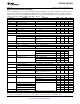
LM25066I, LM25066IA SNVS824C – JUNE 2012 – REVISED MARCH 2013 www.ti.com Table 1. Supported PMBus™ Commands (continued) Function R/W Number Of Data Bytes Default Value READ_VIN Retrieves input voltage measurement. R 2 0000h READ_IIN Retrieves input current measurement (Mirror at D1h). R 2 0000h Code Name 88h 89h 32 8Bh READ_VOUT Retrieves output voltage measurement. R 2 0000h 8Dh READ_TEMPERATURE_1 Retrieves temperature measurement.
LM25066I, LM25066IA www.ti.com SNVS824C – JUNE 2012 – REVISED MARCH 2013 Table 1. Supported PMBus™ Commands (continued) Code Name Function R/W Number Of Data Bytes E0h MFR_SPECIFIC_16 BLACK_BOX_READ Captures diagnostic and telemetry information which are latched when the first SMBA alert occurs after faults have been cleared.
LM25066I, LM25066IA SNVS824C – JUNE 2012 – REVISED MARCH 2013 www.ti.com Table 4. VOUT_UV_WARN_LIMIT Register Value Meaning Default 1h – 0FFFh VOUT Under-voltage Warning detection threshold 0000h (disabled) 0000h VOUT Under-voltage Warning disabled n/a OT_FAULT_LIMIT (4Fh) The OT_FAULT_LIMIT is a standard PMBus™ command that allows configuring or reading the threshold for the Overtemperature Fault detection. Reading and writing to this register should use the coefficients shown in Table 44.
LM25066I, LM25066IA www.ti.com SNVS824C – JUNE 2012 – REVISED MARCH 2013 Table 8. VIN_UV_WARN_LIMIT Register Value Meaning Default 1h – 0FFFh VIN Under-voltage Warning detection threshold 0000h (disabled) 0000h VIN Under-voltage Warning disabled n/a IIN_OC_WARN_LIMIT (5Dh) The IIN_OC_WARN_LIMIT command is a standard PMBus command that allows configuring or reading the threshold for the input current, over current warning. For access to this command use the PMBus Read or Write word protocol.
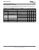
LM25066I, LM25066IA SNVS824C – JUNE 2012 – REVISED MARCH 2013 www.ti.com Table 10. STATUS_WORD Definitions (continued) Bit NAME Meaning Default 1 CML A Communication Fault has occurred 0 0 None of the Above A fault or warning not listed in bits [7:1] has occurred 1 STATUS_VOUT (7Ah) The STATUS_VOUT command is a standard PMBus™ command that returns the value of the VOUT UV Warning flag. Accesses to this command should use the PMBus™ read byte protocol.
LM25066I, LM25066IA www.ti.com SNVS824C – JUNE 2012 – REVISED MARCH 2013 Table 13. STATUS_TEMPERATURE Definitions (continued) Bit NAME Meaning Default 2 reserved Not Supported, always 0 0 1 reserved Not Supported, always 0 0 0 reserved Not Supported, always 0 0 STATUS_CML (7Eh) The STATUS_CML command is a standard PMBus™ command that returns the value of a number of flags related to communication faults. Accesses to this command should use the PMBus™ read byte protocol.
LM25066I, LM25066IA SNVS824C – JUNE 2012 – REVISED MARCH 2013 www.ti.com READ_EIN (86h) The READ_EIN command is a standard PMBus command that returns information the host can use to calculate average input power consumption. Accesses to this command should use the PMBus Block Read protocol. Information provided by this command is independent of any device specific averaging period. Six bytes of data are returned by this command.
LM25066I, LM25066IA www.ti.com SNVS824C – JUNE 2012 – REVISED MARCH 2013 READ_VOUT (8Bh) The READ_VOUT command is a standard PMBus™ command that returns the 12-bit measured value of the output voltage. Reading this register should use the coefficients shown in Table 44. Accesses to this command should use the PMBus™ read word protocol. This value is also used internally for the VOUT Under Voltage Warning detection. Table 18.
LM25066I, LM25066IA SNVS824C – JUNE 2012 – REVISED MARCH 2013 www.ti.com MFR_MODEL (9Ah) The MFR_MODEL command is a standard PMBus™ command that returns the part number of the chip. To read the MFR_MODEL, use the PMBus™ block read protocol. Table 23.
LM25066I, LM25066IA www.ti.com SNVS824C – JUNE 2012 – REVISED MARCH 2013 MFR_SPECIFIC_02: MFR_READ_PIN (D2h) The MFR_ READ_PIN command will report the upper 12 bits of the VIN x IIN product as measured by the 12-bit ADC. To read data from the MFR_READ_PIN command, use the PMBus™ Read Word protocol. Reading this register should use the coefficients shown in Table 44. Please see the section on coefficient calculations to calculate the values to use. Table 27.
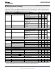
LM25066I, LM25066IA SNVS824C – JUNE 2012 – REVISED MARCH 2013 www.ti.com WARNING Inhibiting the MOSFET switch off in response to over-current or circuit breaker fault conditions will likely result in the destruction of the MOSFET! This functionality should be used with great care and supervision! Table 31.
LM25066I, LM25066IA www.ti.com SNVS824C – JUNE 2012 – REVISED MARCH 2013 MFR_SPECIFIC_09: DEVICE_SETUP (D9h) The DEVICE_SETUP command may be used to override pin settings to define operation of the LM25066I/A under host control. This command is accessed with the PMBus™ read / write byte protocol. Table 33.
LM25066I, LM25066IA SNVS824C – JUNE 2012 – REVISED MARCH 2013 www.ti.com MFR_SPECIFIC_11: SAMPLES_FOR_AVG (DBh) The SAMPLES_FOR_AVERAGE is a manufacturer specific command for setting the number of samples used in computing the average values for IIN, VIN, VOUT, PIN. The decimal equivalent of the AVGN nibble is the power of 2 samples (e.g. AVGN=12 equates to 4096 samples used in computing the average). The LM25066I/A supports average numbers of 1, 2, 4, 8, 16, 32, 64, 128, 256, 512, 1024, 2048, 4096.
LM25066I, LM25066IA www.ti.com SNVS824C – JUNE 2012 – REVISED MARCH 2013 MFR_SPECIFIC_13: READ_AVG_VOUT (DDh) The READ_AVG_VOUT command will report the 12-bit ADC measured average output voltage. The returned value will be the default value (0000h) or previous data when the average data is not ready. This data is read with the PMBus™ Read Word protocol. This register should use the coefficients shown in Table 44. Table 38.
LM25066I, LM25066IA SNVS824C – JUNE 2012 – REVISED MARCH 2013 www.ti.com Table 41.
DIOD E VIN IIN Copyright © 2012–2013, Texas Instruments Incorporated Product Folder Links: LM25066I LM25066IA R EAD _VAUX D 0h PEAK-HOLD C LEAR_PIN_PEAK D6h READ_ PIN_ PEAK D5 h AVERAGED DATA R EAD _VOU T 8Bh CMP CMP CMP CMP CMP CMP CMP CMP CMP PMBus Interface WARNING LIMITS OT_WARNING_LIMIT 51h VOUT_UV_WARN_ LIMIT 4 3h PIN_OP_WAR N_LIMIT D4h IIN _OC_WAR N_LIMIT 5Dh an d D3h VIN _UV_WARN_L IMIT 58 h VIN_ OV_WARN_ LIMIT 57 h MOSFET STATUS C IRC UIT BREAKER MOSFET DISSIPATION L I
LM25066I, LM25066IA SNVS824C – JUNE 2012 – REVISED MARCH 2013 www.ti.com Reading and Writing Telemetry Data and Warning Thresholds All measured telemetry data and user programmed warning thresholds are communicated in 12 bit two’s compliment binary numbers read/written in 2 byte increments conforming to the Direct format as described in section 8.3.3 of the PMBus™ Power System Management Protocol Specification 1.1 (Part II).
LM25066I, LM25066IA www.ti.com SNVS824C – JUNE 2012 – REVISED MARCH 2013 Table 45.
LM25066I, LM25066IA SNVS824C – JUNE 2012 – REVISED MARCH 2013 www.ti.
LM25066I, LM25066IA www.ti.com SNVS824C – JUNE 2012 – REVISED MARCH 2013 Table 47. Device Addressing (continued) ADR2 ADR1 ADR0 Decoded Address 0 1 Z 17h 0 1 0 50h 0 1 1 51h 1 Z Z 52h 1 Z 0 53h 1 Z 1 54h 1 0 Z 55h 1 0 0 56h 1 0 1 57h 1 1 Z 58h 1 1 0 59h 1 1 1 5Ah SMBus Communications Timing Requirements tR SCL tF tLOW VIH VIL tHIGH tHD;DAT tHD;STA tSU;STA tSU;STO tSU;DAT SDA VIH VIL tBUF P S S P Figure 50. SMBus Timing Diagram Table 48.
LM25066I, LM25066IA SNVS824C – JUNE 2012 – REVISED MARCH 2013 www.ti.com Table 48.
LM25066I, LM25066IA www.ti.com SNVS824C – JUNE 2012 – REVISED MARCH 2013 REVISION HISTORY Changes from Revision B (March 2013) to Revision C • Page Changed layout of National Data Sheet to TI format ..........................................................................................................
PACKAGE OPTION ADDENDUM www.ti.
PACKAGE OPTION ADDENDUM www.ti.com 6-Mar-2013 continues to take reasonable steps to provide representative and accurate information but may not have conducted destructive testing or chemical analysis on incoming materials and chemicals. TI and TI suppliers consider certain information to be proprietary, and thus CAS numbers and other limited information may not be available for release.
PACKAGE MATERIALS INFORMATION www.ti.com 26-Mar-2013 TAPE AND REEL INFORMATION *All dimensions are nominal Device Package Package Pins Type Drawing LM25066IAPSQ/NOPB WQFN NHZ 24 LM25066IAPSQE/NOPB WQFN NHZ LM25066IAPSQX/NOPB WQFN NHZ LM25066IPSQ/NOPB WQFN LM25066IPSQE/NOPB LM25066IPSQX/NOPB SPQ Reel Reel A0 Diameter Width (mm) (mm) W1 (mm) B0 (mm) K0 (mm) P1 (mm) W Pin1 (mm) Quadrant 1000 178.0 12.4 4.3 5.3 1.3 8.0 12.0 Q1 24 250 178.0 12.4 4.3 5.3 1.3 8.0 12.
PACKAGE MATERIALS INFORMATION www.ti.com 26-Mar-2013 *All dimensions are nominal Device Package Type Package Drawing Pins SPQ Length (mm) Width (mm) Height (mm) LM25066IAPSQ/NOPB WQFN NHZ 24 1000 213.0 191.0 55.0 LM25066IAPSQE/NOPB WQFN NHZ 24 250 213.0 191.0 55.0 LM25066IAPSQX/NOPB WQFN NHZ 24 4500 367.0 367.0 35.0 LM25066IPSQ/NOPB WQFN NHZ 24 1000 213.0 191.0 55.0 LM25066IPSQE/NOPB WQFN NHZ 24 250 213.0 191.0 55.
MECHANICAL DATA NHZ0024B SQA24B (Rev A) www.ti.
IMPORTANT NOTICE Texas Instruments Incorporated and its subsidiaries (TI) reserve the right to make corrections, enhancements, improvements and other changes to its semiconductor products and services per JESD46, latest issue, and to discontinue any product or service per JESD48, latest issue. Buyers should obtain the latest relevant information before placing orders and should verify that such information is current and complete.