
Datasheet

LM2576, LM2576HV
SNVS107C –JUNE 1999–REVISED APRIL 2013
www.ti.com
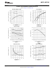
TYPICAL PERFORMANCE CHARACTERISTICS (continued)
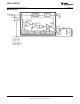
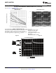
(Circuit of Figure 21 and Figure 22)
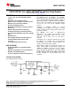
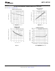
Maximum Power Dissipation
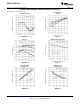
(DDPAK/TO-263) Switching Waveforms
V
OUT
= 15V
If the DDPAK/TO-263 package is used, the thermal resistance can be
A: Output Pin Voltage, 50V/div
reduced by increasing the PC board copper area thermally connected
B: Output Pin Current, 2A/div
to the package. Using 0.5 square inches of copper area, θ
JA
is
C: Inductor Current, 2A/div
50°C/W, with 1 square inch of copper area, θ
JA
is 37°C/W, and with
D: Output Ripple Voltage, 50 mV/div,
1.6 or more square inches of copper area, θ
JA
is 32°C/W.
AC-Coupled
Horizontal Time Base: 5 μs/div
Figure 18. Figure 19.
Load Transient Response
Figure 20.
10 Submit Documentation Feedback Copyright © 1999–2013, Texas Instruments Incorporated
Product Folder Links: LM2576 LM2576HV