
Datasheet

LM2576, LM2576HV
www.ti.com
SNVS107C –JUNE 1999–REVISED APRIL 2013
These devices have limited built-in ESD protection. The leads should be shorted together or the device placed in conductive foam
during storage or handling to prevent electrostatic damage to the MOS gates.
ABSOLUTE MAXIMUM RATINGS
(1)(2)
Maximum Supply Voltage LM2576 45V
LM2576HV 63V
ON /OFF Pin Input Voltage −0.3V ≤ V ≤ +V
IN
Output Voltage to Ground (Steady State) −1V
Power Dissipation Internally Limited
Storage Temperature Range −65°C to +150°C
Maximum Junction Temperature 150°C
Minimum ESD Rating (C = 100 pF, R = 1.5 kΩ) 2 kV
Lead Temperature (Soldering, 10 Seconds) 260°C
(1) Absolute Maximum Ratings indicate limits beyond which damage to the device may occur. Operating Ratings indicate conditions for
which the device is intended to be functional, but do not ensured specific performance limits. For ensured specifications and test
conditions, see ELECTRICAL CHARACTERISTICS ALL OUTPUT VOLTAGE VERSIONS.
(2) If Military/Aerospace specified devices are required, please contact the TI Sales Office/ Distributors for availability and specifications.
OPERATING RATINGS
Temperature Range LM2576/LM2576HV −40°C ≤ T
J
≤ +125°C
Supply Voltage LM2576 40V
LM2576HV 60V
ELECTRICAL CHARACTERISTICS LM2576-3.3, LM2576HV-3.3
Specifications with standard type face are for T
J
= 25°C, and those with boldface type apply over full Operating Temperature
Range.
LM2576-3.3
Units
LM2576HV-3.3
Symbol Parameter Conditions
(Limits)
Typ Limit
(1)
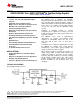
SYSTEM PARAMETERS Test Circuit Figure 21 and Figure 22
(2)
V
OUT
Output Voltage V
IN
= 12V, I
LOAD
= 0.5A 3.3 V
Circuit of Figure 21 and Figure 22 3.234 V(Min)
3.366 V(Max)
V
OUT
Output Voltage 6V ≤ V
IN
≤ 40V, 0.5A ≤ I
LOAD
≤ 3A 3.3 V
LM2576 Circuit of Figure 21 and Figure 22 3.168/3.135 V(Min)
3.432/3.465 V(Max)
V
OUT
Output Voltage 6V ≤ V
IN
≤ 60V, 0.5A ≤ I
LOAD
≤ 3A 3.3 V
LM2576HV Circuit of Figure 21 and Figure 22 3.168/3.135 V(Min)
3.450/3.482 V(Max)
η Efficiency V
IN
= 12V, I
LOAD
= 3A 75 %
(1) All limits specified at room temperature (standard type face) and at temperature extremes (bold type face). All room temperature limits
are 100% production tested. All limits at temperature extremes are specified via correlation using standard Statistical Quality Control
(SQC) methods.
(2) External components such as the catch diode, inductor, input and output capacitors can affect switching regulator system performance.
When the LM2576/LM2576HV is used as shown in Figure 21 and Figure 22, system performance will be as shown in ELECTRICAL
CHARACTERISTICS ALL OUTPUT VOLTAGE VERSIONS.
Copyright © 1999–2013, Texas Instruments Incorporated Submit Documentation Feedback 3
Product Folder Links: LM2576 LM2576HV