
Datasheet
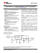

LM2576, LM2576HV
SNVS107C –JUNE 1999–REVISED APRIL 2013
www.ti.com
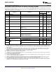
ELECTRICAL CHARACTERISTICS ALL OUTPUT VOLTAGE VERSIONS
Specifications with standard type face are for T
J
= 25°C, and those with boldface type apply over full Operating Temperature
Range. Unless otherwise specified, V
IN
= 12V for the 3.3V, 5V, and Adjustable version, V
IN
= 25V for the 12V version, and V
IN
= 30V for the 15V version. I
LOAD
= 500 mA.
LM2576-XX
Units
LM2576HV-XX
Symbol Parameter Conditions
(Limits)
Typ Limit
(1)
DEVICE PARAMETERS
I
b
Feedback Bias Current V
OUT
= 5V (Adjustable Version Only) 50 100/500 nA
f
O
Oscillator Frequency See
(2)
52 kHz
47/42 kHz (Min)
58/63 kHz (Max)
V
SAT
Saturation Voltage I
OUT
= 3A
(3)
1.4 V
1.8/2.0 V(Max)
DC Max Duty Cycle (ON) See
(4)
98 %
93 %(Min)
I
CL
Current Limit See
(3)(2)
5.8 A
4.2/3.5 A(Min)
6.9/7.5 A(Max)
I
L
Output Leakage Current Output = 0V 2 mA(Max)
Output = −1V 7.5 mA
Output = −1V
(5)(6)
30 mA(Max)
I
Q
Quiescent Current See
(5)
5 mA
10 mA(Max)
I
STBY
Standby Quiescent ON /OFF Pin = 5V (OFF) 50 μA
Current 200 μA(Max)
θ
JA
Thermal Resistance T Package, Junction to Ambient
(7)
65
θ
JA
T Package, Junction to Ambient
(8)
45
°C/W
θ
JC
T Package, Junction to Case 2
θ
JA
S Package, Junction to Ambient
(9)
50
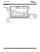
ON /OFF CONTROL Test Circuit Figure 21 and Figure 22
V
IH
ON /OFF Pin V
OUT
= 0V 1.4 2.2/2.4 V(Min)
Logic Input Level
V
IL
V
OUT
= Nominal Output Voltage 1.2 1.0/0.8 V(Max)
I
IH
ON /OFF Pin Input ON /OFF Pin = 5V (OFF) 12 μA
Current 30 μA(Max)
I
IL
ON /OFF Pin = 0V (ON) 0 μA
10 μA(Max)
(1) All limits specified at room temperature (standard type face) and at temperature extremes (bold type face). All room temperature limits
are 100% production tested. All limits at temperature extremes are specified via correlation using standard Statistical Quality Control
(SQC) methods.
(2) The oscillator frequency reduces to approximately 11 kHz in the event of an output short or an overload which causes the regulated
output voltage to drop approximately 40% from the nominal output voltage. This self protection feature lowers the average power
dissipation of the IC by lowering the minimum duty cycle from 5% down to approximately 2%.
(3) Output pin sourcing current. No diode, inductor or capacitor connected to output.
(4) Feedback pin removed from output and connected to 0V.
(5) Feedback pin removed from output and connected to +12V for the Adjustable, 3.3V, and 5V versions, and +25V for the 12V and 15V
versions, to force the output transistor OFF.
(6) V
IN
= 40V (60V for high voltage version).
(7) Junction to ambient thermal resistance (no external heat sink) for the 5 lead TO-220 package mounted vertically, with ½ inch leads in a
socket, or on a PC board with minimum copper area.
(8) Junction to ambient thermal resistance (no external heat sink) for the 5 lead TO-220 package mounted vertically, with ¼ inch leads
soldered to a PC board containing approximately 4 square inches of copper area surrounding the leads.
(9) If the DDPAK/TO-263 package is used, the thermal resistance can be reduced by increasing the PC board copper area thermally
connected to the package. Using 0.5 square inches of copper area, θ
JA
is 50°C/W, with 1 square inch of copper area, θ
JA
is 37°C/W,
and with 1.6 or more square inches of copper area, θ
JA
is 32°C/W.
6 Submit Documentation Feedback Copyright © 1999–2013, Texas Instruments Incorporated
Product Folder Links: LM2576 LM2576HV