LM1577, LM2577 www.ti.com SNOS658D – JUNE 1999 – REVISED APRIL 2013 LM1577/LM2577 SIMPLE SWITCHER® Step-Up Voltage Regulator Check for Samples: LM1577, LM2577 FEATURES DESCRIPTION • • • • The LM1577/LM2577 are monolithic integrated circuits that provide all of the power and control functions for step-up (boost), flyback, and forward converter switching regulators. The device is available in three different output voltage versions: 12V, 15V, and adjustable.
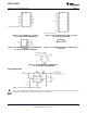
LM1577, LM2577 SNOS658D – JUNE 1999 – REVISED APRIL 2013 www.ti.com *No Internal Connection *No internal Connection Figure 3. 16-Lead PDIP (N) – Top View See Package Number NBG0016G Figure 4. 24-Lead SOIC Package (M) – Top View See Package Number DW Figure 5. 5-Lead DDPAK/TO-263 (S) SFM Package – Figure 6. 5-Lead DDPAK/TO-263 (S) SFM Package – Top View Side View See Package Number KTT0005B Figure 7.
LM1577, LM2577 www.ti.com SNOS658D – JUNE 1999 – REVISED APRIL 2013 Absolute Maximum Ratings (1) (2) Supply Voltage 45V Output Switch Voltage 65V Output Switch Current (3) 6.0A Power Dissipation Internally Limited −65°C to +150°C Storage Temperature Range Lead Temperature Soldering, 10 sec. 260°C Maximum Junction Temperature Minimum ESD Rating (1) (2) (3) 150°C C = 100 pF, R = 1.5 kΩ 2 kV Absolute Maximum Ratings indicate limits beyond which damage to the device may occur.
LM1577, LM2577 SNOS658D – JUNE 1999 – REVISED APRIL 2013 www.ti.com Electrical Characteristics—LM1577-12, LM2577-12 (continued) Specifications with standard type face are for TJ = 25°C, and those in bold type face apply over full Operating Temperature Range. Unless otherwise specified, VIN = 5V, and ISWITCH = 0.
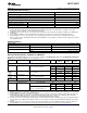
LM1577, LM2577 www.ti.com SNOS658D – JUNE 1999 – REVISED APRIL 2013 Electrical Characteristics—LM1577-15, LM2577-15 Specifications with standard type face are for TJ = 25°C, and those in bold type face apply over full Operating Temperature Range. Unless otherwise specified, VIN = 5V, and ISWITCH = 0. Symbol Parameter Conditions Typical LM1577-15 Limit (1) (2) LM2577-15 Limit (3) Units (Limits) 14.50/14.25 14.50/14.25 V(min) 15.50/15.75 15.50/15.
LM1577, LM2577 SNOS658D – JUNE 1999 – REVISED APRIL 2013 www.ti.com Electrical Characteristics—LM1577-15, LM2577-15 (continued) Specifications with standard type face are for TJ = 25°C, and those in bold type face apply over full Operating Temperature Range. Unless otherwise specified, VIN = 5V, and ISWITCH = 0. Symbol Parameter Error Amplifier Output Swing Error Amp Output Current ISS D Soft Start Current Maximum Duty Cycle Conditions Upper Limit VFEEDBACK = 12.0V 2.4 Lower Limit VFEEDBACK = 18.
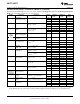
LM1577, LM2577 www.ti.com SNOS658D – JUNE 1999 – REVISED APRIL 2013 Electrical Characteristics—LM1577-ADJ, LM2577-ADJ Specifications with standard type face are for TJ = 25°C, and those in bold type face apply over full Operating Temperature Range. Unless otherwise specified, VIN = 5V, VFEEDBACK = VREF, and ISWITCH = 0.
LM1577, LM2577 SNOS658D – JUNE 1999 – REVISED APRIL 2013 www.ti.com Electrical Characteristics—LM1577-ADJ, LM2577-ADJ (continued) Specifications with standard type face are for TJ = 25°C, and those in bold type face apply over full Operating Temperature Range. Unless otherwise specified, VIN = 5V, VFEEDBACK = VREF, and ISWITCH = 0. Symbol ISS D Parameter Conditions Error Amp Output Current VFEEDBACK = 1.0V to 1.5V VCOMP = 1.0V Soft Start Current VFEEDBACK = 1.
LM1577, LM2577 www.ti.com SNOS658D – JUNE 1999 – REVISED APRIL 2013 Typical Performance Characteristics Reference Voltage vs Temperature Reference Voltage vs Temperature Figure 8. Figure 9. Reference Voltage vs Temperature Δ Reference Voltage vs Supply Voltage Figure 10. Figure 11. Δ Reference Voltage vs Supply Voltage Δ Reference Voltage vs Supply Voltage Figure 12. Figure 13.
LM1577, LM2577 SNOS658D – JUNE 1999 – REVISED APRIL 2013 www.ti.com Typical Performance Characteristics (continued) 10 Error Amp Transconductance vs Temperature Error Amp Transconductance vs Temperature Figure 14. Figure 15. Error Amp Transconductance vs Temperature Error Amp Voltage Gain vs Temperature Figure 16. Figure 17. Error Amp Voltage Gain vs Temperature Error Amp Voltage Gain vs Temperature Figure 18. Figure 19.
LM1577, LM2577 www.ti.com SNOS658D – JUNE 1999 – REVISED APRIL 2013 Typical Performance Characteristics (continued) Quiescent Current vs Temperature Quiescent Current vs Switch Current Figure 20. Figure 21. Current Limit vs Temperature Current Limit Response Time vs Overdrive Figure 22. Figure 23. Switch Saturation Voltage vs Switch Current Switch Transconductance vs Temperature Figure 24. Figure 25.
LM1577, LM2577 SNOS658D – JUNE 1999 – REVISED APRIL 2013 www.ti.com Typical Performance Characteristics (continued) Feedback Pin Bias Current vs Temperature Oscillator Frequency vs Temperature Figure 26. Figure 27. Maximum Power Dissipation (DDPAK/TO-263) (1) Figure 28. (1) 12 If the DDPAK/TO-263 package is used, the thermal resistance can be reduced by increasing the PC board copper area thermally connected to the package. Using 0.
LM1577, LM2577 www.ti.com SNOS658D – JUNE 1999 – REVISED APRIL 2013 LM1577-12, LM2577-12 TEST CIRCUIT L = 415-0930 (AIE) D = any manufacturer COUT = Sprague Type 673D Electrolytic 680 μF, 20V Note: Pin numbers shown are for TO-220 (T) package Figure 29. Circuit Used to Specify System Parameters for 12V Versions LM1577-15, LM2577-15 Test Circuit L = 415-0930 (AIE) D = any manufacturer COUT = Sprague Type 673D Electrolytic 680 μF, 20V Note: Pin numbers shown are for TO-220 (T) package Figure 30.
LM1577, LM2577 SNOS658D – JUNE 1999 – REVISED APRIL 2013 www.ti.com LM1577-ADJ, LM2577-ADJ Test Circuit L = 415-0930 (AIE) D = any manufacturer COUT = Sprague Type 673D Electrolytic 680 μF, 20V R1 = 48.7k in series with 511Ω (1%) R2 = 5.62k (1%) Note: Pin numbers shown are for TO-220 (T) package Figure 31. Circuit Used to Specify System Parameters for ADJ Versions Application Hints Note: Pin numbers shown are for TO-220 (T) package *Resistors are internal to LM1577/LM2577 for 12V and 15V versions.
LM1577, LM2577 www.ti.com SNOS658D – JUNE 1999 – REVISED APRIL 2013 STEP-UP (BOOST) REGULATOR Figure 32 shows the LM1577-ADJ/LM2577-ADJ used as a Step-Up Regulator. This is a switching regulator used for producing an output voltage greater than the input supply voltage. The LM1577-12/LM2577-12 and LM157715/LM2577-15 can also be used for step-up regulators with 12V or 15V outputs (respectively), by tying the feedback pin directly to the regulator output. A basic explanation of how it works is as follows.
LM1577, LM2577 SNOS658D – JUNE 1999 – REVISED APRIL 2013 www.ti.com STEP-UP REGULATOR DESIGN PROCEDURE The following design procedure can be used to select the appropriate external components for the circuit in Figure 32, based on these system requirements.
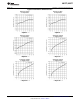
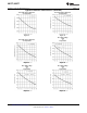
LM1577, LM2577 www.ti.com SNOS658D – JUNE 1999 – REVISED APRIL 2013 2. Find where E•T intersects this inductor value to determine if it has an L or H prefix. If E•T intersects both the L and H regions, select the inductor with an H prefix. Figure 34. LM2577-12 Inductor Selection Guide Figure 35.
LM1577, LM2577 SNOS658D – JUNE 1999 – REVISED APRIL 2013 www.ti.com Note: These charts assume that the inductor ripple current is approximately 20% to 30% of the average inductor current (when the regulator is under full load). Greater ripple current causes higher peak switch currents and greater output ripple voltage; lower ripple current is achieved with larger-value inductors. The factor of 20 to 30% is chosen as a convenient balance between the two extremes. Figure 36.
LM1577, LM2577 www.ti.com SNOS658D – JUNE 1999 – REVISED APRIL 2013 Table 2.
LM1577, LM2577 SNOS658D – JUNE 1999 – REVISED APRIL 2013 www.ti.com The compensation capacitor is also part of the soft start circuitry. When power to the regulator is turned on, the switch duty cycle is allowed to rise at a rate controlled by this capacitor (with no control on the duty cycle, it would immediately rise to 90%, drawing huge currents from the input power supply). In order to operate properly, the soft start circuit requires CC ≥ 0.22 μF.
LM1577, LM2577 www.ti.com SNOS658D – JUNE 1999 – REVISED APRIL 2013 Table 3. Aluminum Electrolytic Capacitors Recommended for Switching Regulators Cornell Dublier —Types 239, 250, 251, UFT, 300, or 350 P.O.
LM1577, LM2577 SNOS658D – JUNE 1999 – REVISED APRIL 2013 www.ti.com Note: Pin numbers shown are for TO-220 (T) package. Figure 37. Step-up Regulator Delivers 12V from a 5V Input Figure 38. Line Regulation (Typical) of Step-Up Regulator of Figure 37 A: Output Voltage Change, 100 mV/div. (AC-coupled) B: Load current, 0.2 A/div Horizontal: 5 ms/div Figure 39.
LM1577, LM2577 www.ti.com SNOS658D – JUNE 1999 – REVISED APRIL 2013 A: Switch pin voltage, 10 V/div B: Switch pin current, 2 A/div C: Inductor current, 2 A/div D: Output ripple voltage, 100 mV/div (AC-coupled) Horizontal: 5 μs/div Figure 40. Switching Waveforms of Step-Up Regulator of Figure 37 FLYBACK REGULATOR A Flyback regulator can produce single or multiple output voltages that are lower or greater than the input supply voltage.
LM1577, LM2577 SNOS658D – JUNE 1999 – REVISED APRIL 2013 www.ti.com (15) Where ∑ILOAD(max) is the sum of the load current (magnitude) required from both outputs. Select a resistor less than or equal to this value, and no greater than 3 kΩ. B. Calculate the minimum value for ∑COUT (sum of COUT at both outputs) using the following two equations. (16) The larger of these two values must be used to ensure regulator stability. Figure 41.
LM1577, LM2577 www.ti.com SNOS658D – JUNE 1999 – REVISED APRIL 2013 Table 5. Flyback Regulator Formulas (continued) Peak Primary Current IP(PK) Switch Voltage when Off (19) VSW(OFF) (20) Diode Reverse Voltage VR VOUT+ N (VIN− VSAT) Average Diode Current ID(AVE) ILOAD Peak Diode Current ID(PK) (21) Short Circuit Diode Current (22) Power Dissipation of LM1577/LM2577 PD (23) C. Calculate the minimum value of CC (24) D.
LM1577, LM2577 SNOS658D – JUNE 1999 – REVISED APRIL 2013 www.ti.com The primary of a flyback transformer draws discontinuous pulses of current from the input supply. As a result, a flyback regulator generates more noise at the input supply than a step-up regulator, and this requires a larger bypass capacitor to decouple the LM1577/LM2577 VIN pin from this noise. For most applications, a low ESR, 1.0 μF cap will be sufficient, if it is connected very close to the VIN and Ground pins.
LM1577, LM2577 www.ti.com SNOS658D – JUNE 1999 – REVISED APRIL 2013 Figure 43. Snubber Circuit FLYBACK REGULATOR CIRCUIT EXAMPLE The circuit of Figure 44 produces ±15V (at 225 mA each) from a single 5V input. The output regulation of this circuit is shown in Figure 45 and Figure 47, while the load transient response is shown in Figure 46 and Figure 48. Switching waveforms seen in this circuit are shown in Figure 49. T1 = Pulse Engineering, PE-65300 D1, D2 = 1N5821 Figure 44.
LM1577, LM2577 SNOS658D – JUNE 1999 – REVISED APRIL 2013 www.ti.com A: Output Voltage Change, 100 mV/div B: Output Current, 100 mA/div Horizontal: 10 ms/div Figure 46. Load Transient Response of Flyback Regulator of Figure 44, +15V Output Figure 47.
LM1577, LM2577 www.ti.com SNOS658D – JUNE 1999 – REVISED APRIL 2013 A: Output Voltage Change, 100 mV/div B: Output Current, 100 mA/div Horizontal: 10 ms/div Figure 48. Load Transient Response of Flyback Regulator of Figure 44, −15V Output A: Switch pin voltage, 20 V/div B: Primary current, 2 A/div C: +15V Secondary current, 1 A/div D: +15V Output ripple voltage, 100 mV/div Horizontal: 5 μs/div Figure 49.
LM1577, LM2577 SNOS658D – JUNE 1999 – REVISED APRIL 2013 www.ti.com REVISION HISTORY Changes from Revision C (April 2013) to Revision D • 30 Page Changed layout of National Data Sheet to TI format ..........................................................................................................
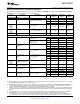
PACKAGE OPTION ADDENDUM www.ti.
PACKAGE OPTION ADDENDUM www.ti.
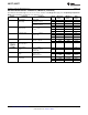
PACKAGE OPTION ADDENDUM www.ti.com 1-Nov-2013 (5) Multiple Device Markings will be inside parentheses. Only one Device Marking contained in parentheses and separated by a "~" will appear on a device. If a line is indented then it is a continuation of the previous line and the two combined represent the entire Device Marking for that device. (6) Lead/Ball Finish - Orderable Devices may have multiple material finish options. Finish options are separated by a vertical ruled line.
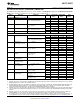
PACKAGE MATERIALS INFORMATION www.ti.com 23-Sep-2013 TAPE AND REEL INFORMATION *All dimensions are nominal Device Package Package Pins Type Drawing SPQ Reel Reel A0 Diameter Width (mm) (mm) W1 (mm) B0 (mm) K0 (mm) P1 (mm) W Pin1 (mm) Quadrant LM2577SX-12/NOPB DDPAK/ TO-263 KTT 5 500 330.0 24.4 10.75 14.85 5.0 16.0 24.0 Q2 LM2577SX-ADJ DDPAK/ TO-263 KTT 5 500 330.0 24.4 10.75 14.85 5.0 16.0 24.0 Q2 LM2577SX-ADJ/NOPB DDPAK/ TO-263 KTT 5 500 330.0 24.4 10.75 14.
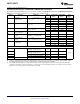
PACKAGE MATERIALS INFORMATION www.ti.com 23-Sep-2013 *All dimensions are nominal Device Package Type Package Drawing Pins SPQ Length (mm) Width (mm) Height (mm) LM2577SX-12/NOPB DDPAK/TO-263 KTT 5 500 367.0 367.0 45.0 LM2577SX-ADJ DDPAK/TO-263 KTT 5 500 367.0 367.0 45.0 LM2577SX-ADJ/NOPB DDPAK/TO-263 KTT 5 500 367.0 367.0 45.
MECHANICAL DATA NDH0005D www.ti.
MECHANICAL DATA NBG0016G www.ti.
MECHANICAL DATA KTT0005B TS5B (Rev D) BOTTOM SIDE OF PACKAGE www.ti.
MECHANICAL DATA NEB0005B www.ti.
IMPORTANT NOTICE Texas Instruments Incorporated and its subsidiaries (TI) reserve the right to make corrections, enhancements, improvements and other changes to its semiconductor products and services per JESD46, latest issue, and to discontinue any product or service per JESD48, latest issue. Buyers should obtain the latest relevant information before placing orders and should verify that such information is current and complete.