LM2593HV LM2593HV SIMPLE SWITCHERPower Converter 150 kHz 2A Step-Down Voltage Regulator, with Features Literature Number: SNVS082D
LM2593HV SIMPLE SWITCHER ® Power Converter 150 kHz 2A Step-Down Voltage Regulator, with Features General Description Features The LM2593HV series of regulators are monolithic integrated circuits that provide all the active functions for a step-down (buck) switching regulator, capable of driving a 2A load with excellent line and load regulation. These devices are available in fixed output voltages of 3.3V, 5V, and an adjustable output version.
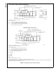
LM2593HV Absolute Maximum Ratings ESD Susceptibility (Note 1) Human Body Model (Note 3) If Military/Aerospace specified devices are required, please contact the National Semiconductor Sales Office/ Distributors for availability and specifications. Maximum Supply Voltage (VIN) S Package 63V SD /SS Pin Input Voltage (Note 2) 6V Delay Pin Voltage (Note 2) 1.5V +215˚C Infrared (10 sec.) +245˚C +260˚C Maximum Junction Temperature +150˚C −0.
(Continued) Specifications with standard type face are for TJ = 25˚C, and those with boldface type apply over full Operating Temperature Range. Symbol η Parameter Efficiency Conditions LM2593HV-ADJ Units (Limits) Typ Limit (Note 4) (Note 5) VIN = 12V, VOUT = 3V, ILOAD = 2A 75 % All Output Voltage Versions Electrical Characteristics Specifications with standard type face are for TJ = 25˚C, and those with boldface type apply over full Operating Temperature Range.
LM2593HV All Output Voltage Versions Electrical Characteristics (Continued) Specifications with standard type face are for TJ = 25˚C, and those with boldface type apply over full Operating Temperature Range. Unless otherwise specified, VIN = 12V for the 3.3V, 5V, and Adjustable version.
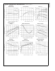
Normalized Output Voltage (Circuit of Figure 1) Line Regulation 10133302 Switch Saturation Voltage Efficiency 10133303 Switch Current Limit 10133304 Dropout Voltage 10133306 10133305 Operating Quiescent Current LM2593HV Typical Performance Characteristics Shutdown Quiescent Current 10133308 Minimum Operating Supply Voltage 10133309 5 10133307 10133310 www.national.
LM2593HV Typical Performance Characteristics Feedback Pin Bias Current (Circuit of Figure 1) (Continued) Flag Saturation Voltage 10133311 Switching Frequency Shutdown /Soft-start Current Soft-start 10133314 Soft-start Response 10133313 10133312 10133315 Shutdown/Soft-start Threshold Voltage 10133318 Delay Pin Current 10133316 Internal Gain-Phase Characteristics 10133353 10133378 www.national.
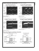
(Circuit of Figure 1) (Continued) Discontinuous Mode Switching Waveforms VIN = 20V, VOUT = 5V, ILOAD = 500 mA L = 10 µH, COUT = 330 µF, COUT ESR = 45 mΩ Continuous Mode Switching Waveforms VIN = 20V, VOUT = 5V, ILOAD = 2A L = 32 µH, COUT = 220 µF, COUT ESR = 50 mΩ 10133320 10133319 Horizontal Time Base: 2 µs/div. Horizontal Time Base: 2 µs/div. A: Output Pin Voltage, 10V/div. A: Output Pin Voltage, 10V/div. B: Inductor Current 1A/div. B: Inductor Current 0.5A/div.
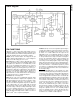
LM2593HV Test Circuit and Layout Guidelines Fixed Output Voltage Versions 10133324 Component Values shown are for VIN = 15V, VOUT = 5V, ILOAD = 2A. CIN — COUT 470 µF, 50V, Aluminum Electrolytic Nichicon “PM Series” — 220 µF, 25V Aluminum Electrolytic, Nichicon “PM Series” D1 — 3.
LM2593HV Block Diagram 10133330 Feedback (Pin 6) — Senses the regulated output voltage to complete the feedback loop. This pin is directly connected to the Output for the fixed voltage versions, but is set to 1.23V by means of a resistive divider from the output for the Adjustable version. If a feedforward capacitor is used (Adjustable version), then a negative voltage spike is generated on this pin whenever the output is shorted.
LM2593HV PIN FUNCTIONS (Continued) Note If any of the above three features (Shutdown /Soft-start, Error Flag, or Delay) are not used, the respective pins can be left open. 10133331 FIGURE 2. Soft-Start, Delay, Error Output www.national.
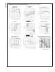
LM2593HV 10133332 FIGURE 3. Timing Diagram for 5V Output INDUCTOR VALUE SELECTION GUIDES (For Continuous Mode Operation) 10133365 FIGURE 4. LM2593HV-3.3 11 www.national.
LM2593HV INDUCTOR VALUE SELECTION GUIDES (For Continuous Mode Operation) (Continued) 10133366 FIGURE 5. LM2593HV-5.0 10133367 FIGURE 6. LM2593HV-ADJ www.national.
(For Continuous Mode Operation) (Continued) 10133368 FIGURE 7. Current Ripple Ratio Coilcraft Inc. Coilcraft Inc., Europe Pulse Engineering Inc. Phone (USA): 1-800-322-2645 Web Address http://www.coilcraft.com Phone (UK): 1-236-730595 Web Address http://www.coilcraft-europe.com Phone (USA): 1-858-674-8100 Web Address http://www.pulseeng.com Pulse Engineering Inc., Phone (UK): 1-483-401700 Europe Web Address http://www.pulseeng.com Renco Electronics Inc.
LM2593HV Application Information INDUCTOR SELECTION PROCEDURE Application Note AN-1197 titled ’Selecting Inductors for Buck Converters’ provides detailed information on this topic. For a quick-start the designer may refer to the nomographs provided in Figure 4 to Figure 6.
input capacitor, this capacitor should be chosen for its RMS current rating rather than its capacitance or voltage ratings, although the capacitance value and voltage rating are directly related to the RMS current rating. The voltage rating of the capacitor and its RMS ripple current capability must never be exceeded. (Continued) OUTPUT CAPACITOR COUT — An output capacitor is required to filter the output and provide regulator loop stability.
LM2593HV Application Information (Continued) 10133342 FIGURE 9. Typical Circuit Using Shutdown /Soft-start and Error Flag Features 10133343 FIGURE 10. Inverting −5V Regulator With Shutdown and Soft-start lNVERTING REGULATOR The circuit in Figure 10 converts a positive input voltage to a negative output voltage with a common ground.
LM2593HV Application Information (Continued) suming 100% efficiency, which is never so. Therefore expect IPEAK to be an additional 10-20% higher than calculated from the above equation. The reader is also referred to Application Note AN-1157 for examples based on positive to negative configuration. The maximum voltage appearing across the regulator is the absolute sum of the input and output voltage, and this must be limited to a maximum of 60V.
LM2593HV Application Information This method of generating a negative output voltage without an additional inductor can be used with other members of the Simple Switcher Family, using either the buck or boost topology. (Continued) on the regulated positive output for the charge pump to work correctly. Also, resistor R1 is required to limit the charging current of C1 to some value less than the LM2593HV current limit. 10133348 FIGURE 14.
LM2593HV Application Information (Continued) 10133338 FIGURE 15. Junction Temperature Rise, TO-263 Layout Suggestions As in any switching regulator, layout is very important. Rapidly switching currents associated with wiring inductance can generate voltage transients which can cause problems. For minimal inductance and ground loops, with reference to Figure 1, the wires indicated by heavy lines should be wide printed circuit traces and should be kept as short as possible.
LM2593HV Physical Dimensions inches (millimeters) unless otherwise noted 7-Lead TO-220 Bent and Staggered Package Order Number LM2593HVT-3.3, LM2593HVT-5.0 or LM2593HVT-ADJ NS Package Number TA07B www.national.
inches (millimeters) unless otherwise noted (Continued) 7-Lead TO-263 Bent and Formed Package Order Number LM2593HVS-3.3, LM2593HVS-5.0 or LM2593HVS-ADJ NS Package Number TS7B LIFE SUPPORT POLICY NATIONAL’S PRODUCTS ARE NOT AUTHORIZED FOR USE AS CRITICAL COMPONENTS IN LIFE SUPPORT DEVICES OR SYSTEMS WITHOUT THE EXPRESS WRITTEN APPROVAL OF THE PRESIDENT AND GENERAL COUNSEL OF NATIONAL SEMICONDUCTOR CORPORATION. As used herein: 1.
IMPORTANT NOTICE Texas Instruments Incorporated and its subsidiaries (TI) reserve the right to make corrections, modifications, enhancements, improvements, and other changes to its products and services at any time and to discontinue any product or service without notice. Customers should obtain the latest relevant information before placing orders and should verify that such information is current and complete.