
Datasheet

LM2594, LM2594HV
www.ti.com
SNVS118C –DECEMBER 1999–REVISED APRIL 2013
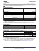
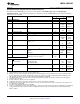
All Output Voltage Versions Electrical Characteristics
Specifications with standard type face are for T
J
= 25°C, and those with boldface type apply over full Operating
Temperature Range . Unless otherwise specified, V
IN
= 12V for the 3.3V, 5V, and Adjustable version and V
IN
= 24V for the
12V version. I
LOAD
= 100 mA
Symbol Parameter Conditions LM2594/LM2594HV-XX Units
(Limits)
Typ
(1)
Limit
(2)
DEVICE PARAMETERS
I
b
Feedback Bias Current Adjustable Version Only, VFB = 1.3V 10 50/100 nA
f
O
Oscillator Frequency See
(3)
150 kHz
127/110 kHz(min)
173/173 kHz(max)
V
SAT
Saturation Voltage I
OUT
= 0.5A
(4)(5)
0.9 V
1.1/1.2 V(max)
DC Max Duty Cycle (ON) See
(5)
100 %
Min Duty Cycle (OFF) See
(6)
0
I
CL
Current Limit Peak Current
(4)(5)
0.8 A
0.65/0.58 A(min)
1.3/1.4 A(max)
I
L
Output Leakage Current Output = 0V
(4)(6)(7)
50 μA(max)
Output = −1V
2 mA
15 mA(max)
I
Q
Quiescent Current See
(6)
5 mA
10 mA(max)
I
STBY
Standby Quiescent Current ON/OFF pin = 5V (OFF)
(7)
85 μA
LM2594 200/250 μA(max)
LM2594HV 140 250/300 μA(max)
θ
JA
Thermal Resistance P Package, Junction to Ambient
(8)
95 °C/W
MDPackage, Junction to Ambient
(8)
150
ON/OFF CONTROL Test Circuit Figure 20
ON /OFF Pin Logic Input 1.3 V
V
IH
Threshold Voltage Low (Regulator ON) 0.6 V(max)
V
IL
High (Regulator OFF) 2.0 V(min)
I
H
ON /OFF Pin Input Current V
LOGIC
= 2.5V (Regulator OFF) 5 μA
15 μA(max)
I
L
V
LOGIC
= 0.5V (Regulator ON) 0.02 μA
5 μA(max)
(1) Typical numbers are at 25°C and represent the most likely norm.
(2) All limits ensured at room temperature (standard type face) and at temperature extremes (bold type face). All room temperature limits
are 100% production tested. All limits at temperature extremes are specified via correlation using standard Statistical Quality Control
(SQC) methods. All limits are used to calculate Average Outgoing Quality Level (AOQL).
(3) The switching frequency is reduced when the second stage current limit is activated. The amount of reduction is determined by the
severity of current overload.
(4) No diode, inductor or capacitor connected to output pin.
(5) Feedback pin removed from output and connected to 0V to force the output transistor switch ON.
(6) Feedback pin removed from output and connected to 12V for the 3.3V, 5V, and the ADJ. version, and 15V for the 12V version, to force
the output transistor switch OFF.
(7) V
IN
= 40V for the LM2594 and 60V for the LM2594HV.
(8) Junction to ambient thermal resistance with approximately 1 square inch of printed circuit board copper surrounding the leads. Additional
copper area will lower thermal resistance further. See application hints in this data sheet and the thermal model in Switchers Made
Simple
®
software.
Copyright © 1999–2013, Texas Instruments Incorporated Submit Documentation Feedback 5
Product Folder Links: LM2594 LM2594HV