
Datasheet

LM2595
SNVS122B –MAY 1999–REVISED APRIL 2013
www.ti.com
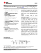
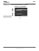
Figure 1. Bent and Staggered Leads, Through
Hole Package
5–Lead TO-220 (NDH)
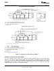
Figure 3. 16-Lead Ceramic Dual-in-Line Package
(NFE)
Figure 2. Surface Mount Package
5-Lead TO-263 (KTT)
These devices have limited built-in ESD protection. The leads should be shorted together or the device placed in conductive foam
during storage or handling to prevent electrostatic damage to the MOS gates.
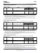
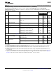
Absolute Maximum Ratings
(1)(2)
Maximum Supply Voltage 45V
ON /OFF Pin Input Voltage −0.3 ≤ V ≤ +25V
Feedback Pin Voltage −0.3 ≤ V ≤ +25V
Output Voltage to Ground
(Steady State) −1V
Power Dissipation Internally limited
Storage Temperature Range −65°C to +150°C
ESD Susceptibility
Human Body Model
(3)
2 kV
Lead Temperature
KTT Package
Vapor Phase (60 sec.) +215°C
Infrared (10 sec.) +245°C
NDH Package (Soldering, 10 sec.) +260°C
Maximum Junction Temperature +150°C
(1) Absolute Maximum Ratings indicate limits beyond which damage to the device may occur. Operating Ratings indicate conditions for
which the device is intended to be functional, but do not ensure specific performance limits. For ensured specifications and test
conditions, see the Electrical Characteristics.
(2) If Military/Aerospace specified devices are required, please contact the Texas Instruments Sales Office/ Distributors for availability and
specifications.
(3) The human body model is a 100 pF capacitor discharged through a 1.5k resistor into each pin.
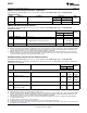
Operating Conditions
Temperature Range −40°C ≤ T
J
≤ +125°C
Supply Voltage 4.5V to 40V
2 Submit Documentation Feedback Copyright © 1999–2013, Texas Instruments Incorporated
Product Folder Links: LM2595