
Datasheet

LM2595
SNVS122B –MAY 1999–REVISED APRIL 2013
www.ti.com
LM2595-12 Electrical Characteristics (continued)
Specifications with standard type face are for T
J
= 25°C, and those with boldface type apply over full Operating
Temperature Range.
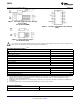
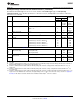
Symbol Parameter Conditions LM2595-12 Units
(Limits)
Typ Limit
(1) (2)
η Efficiency V
IN
= 25V, I
LOAD
= 1A 90 %
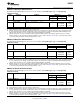
LM2595-ADJ Electrical Characteristics
Specifications with standard type face are for T
J
= 25°C, and those with boldface type apply over full Operating
Temperature Range.
Symbol Parameter Conditions LM2595-ADJ Units
(Limits)
Typ Limit
(1) (2)
SYSTEM PARAMETERS
(3)
Test Circuit Figure 21
V
FB
Feedback Voltage 4.5V ≤ V
IN
≤ 40V, 0.1A ≤ I
LOAD
≤ 1A 1.230 V
V
OUT
programmed for 3V. Circuit of Figure 21 1.193/1.180 V(min)
1.267/1.280 V(max)
η Efficiency V
IN
= 12V, V
OUT
= 3V, I
LOAD
= 1A 78 %
(1) Typical numbers are at 25°C and represent the most likely norm.
(2) All limits specified at room temperature (standard type face) and at temperature extremes (bold type face). All room temperature limits
are 100% production tested. All limits at temperature extremes are specified via correlation using standard Statistical Quality Control
(SQC) methods. All limits are used to calculate Average Outgoing Quality Level (AOQL).
(3) External components such as the catch diode, inductor, input and output capacitors, and voltage programming resistors can affect
switching regulator system performance. When the LM2595 is used as shown in the Figure 21 test circuit, system performance will be
as shown in system parameters of Electrical Characteristics section.
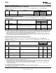
All Output Voltage Versions Electrical Characteristics
Specifications with standard type face are for T
J
= 25°C, and those with boldface type apply over full Operating
Temperature Range. Unless otherwise specified, V
IN
= 12V for the 3.3V, 5V, and Adjustable version and V
IN
= 24V for the
12V version. I
LOAD
= 200 mA.
Symbol Parameter Conditions LM2595-XX Units
(Limits)
Typ Limit
(1) (2)
DEVICE PARAMETERS
I
b
Feedback Bias Current Adjustable Version Only,V
FB
= 1.3V 10 nA
50/100 nA (max)
f
O
Oscillator Frequency See
(3)
150 kHz
127/110 kHz(min)
173/173 kHz(max)
V
SAT
Saturation Voltage I
OUT
= 1A
(4) (5)
1 V
1.2/1.3 V(max)
DC Max Duty Cycle (ON) See
(5)
100 %
Min Duty Cycle (OFF) See
(6)
0
(1) Typical numbers are at 25°C and represent the most likely norm.
(2) All limits specified at room temperature (standard type face) and at temperature extremes (bold type face). All room temperature limits
are 100% production tested. All limits at temperature extremes are specified via correlation using standard Statistical Quality Control
(SQC) methods. All limits are used to calculate Average Outgoing Quality Level (AOQL).
(3) The switching frequency is reduced when the second stage current limit is activated. The amount of reduction is determined by the
severity of current overload.
(4) No diode, inductor or capacitor connected to output pin.
(5) Feedback pin removed from output and connected to 0V to force the output transistor switch ON.
(6) Feedback pin removed from output and connected to 12V for the 3.3V, 5V, and the ADJ. version, and 15V for the 12V version, to force
the output transistor switch OFF.
4 Submit Documentation Feedback Copyright © 1999–2013, Texas Instruments Incorporated
Product Folder Links: LM2595