
Datasheet
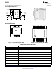
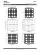

1
16
2
3
4
5
6
7 8
15 14
13 11
12
9 10
20
19 18
17
5
6
7
4
3 2
1
16
15
14
13
9
10 11
12
8
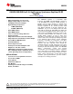
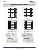
DAP
VIN
PG
1
PG
2
SW
1
SW
2
FB
1
FB
2
GND
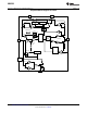
LM26420
V
OUT1
2.5V/2A
Vin
3V to 5.5V
EN
1
EN
2
Buck 1 Buck 2
V
OUT2
1.2V/2A
LM26420
SNVS579F –FEBRUARY 2009–REVISED MARCH 2013
www.ti.com
Typical Application Circuit
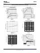
Connection Diagram
Figure 1. 16-Pin WQFN (TOP VIEW) Figure 2. 20-Pin TSSOP (TOP VIEW)
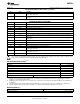
PIN DESCRIPTIONS 20-PIN TSSOP
Pin Name Function
3, 4 VIND
1
Power Input supply for Buck 1.
17, 18 VIND
2
Power Input supply for Buck 2.
1 VINC Input supply for control circuitry.
6,7 PGND
1
Power ground pin for Buck 1.
14, 15 PGND
2
Power ground pin for Buck 2.
20 AGND Signal ground pin. Place the bottom resistor of the feedback network as close as possible to pin.
9 PG
1
Power Good Indicator for Buck 1. Pin is connected through a resistor to an external supply (open
drain output).
12 PG
2
Power Good Indicator for Buck 2. Pin is connected through a resistor to an external supply (open
drain output).
8 FB
1
Feedback pin for Buck 1. Connect to external resistor divider to set output voltage.
13 FB
2
Feedback pin for Buck 2. Connect to external resistor divider to set output voltage.
5 SW
1
Output switch for Buck 1. Connect to the inductor.
16 SW
2
Output switch for Buck 2. Connect to the inductor.
2 EN
1
Enable control input. Logic high enable operation for Buck 1. Do not allow this pin to float or be
greater than VIN + 0.3V.
2 Submit Documentation Feedback Copyright © 2009–2013, Texas Instruments Incorporated
Product Folder Links: LM26420