
Datasheet

LM26420
www.ti.com
SNVS579F –FEBRUARY 2009–REVISED MARCH 2013
PIN DESCRIPTIONS 20-PIN TSSOP (continued)
Pin Name Function
19 EN
2
Enable control input. Logic high enable operation for Buck 2. Do not allow this pin to float or be
greater than VIN + 0.3V.
10, 11, DAP Die Attach Pad Connect to system ground for low thermal impedance, but it cannot be used as a primary GND
connection.
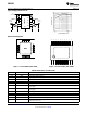
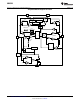
PIN DESCRIPTIONS 16-PIN WQFN
Pin Name Function
1,2 VIND
1
Power Input supply for Buck 1.
11, 12 VIND
2
Power Input supply for Buck 2.
15 VINC Input supply for control circuitry.
4 PGND
1
Power ground pin for Buck 1.
9 PGND
2
Power ground pin for Buck 2.
14 AGND Signal ground pin. Place the bottom resistor of the feedback network as close as possible to pin.
6 PG
1
Power Good Indicator for Buck 1. Pin is connected through a resistor to an external supply (open
drain output).
7 PG
2
Power Good Indicator for Buck 2. Pin is connected through a resistor to an external supply (open
drain output).
5 FB
1
Feedback pin for Buck 1. Connect to external resistor divider to set output voltage.
8 FB
2
Feedback pin for Buck 2. Connect to external resistor divider to set output voltage.
3 SW
1
Output switch for Buck 1. Connect to the inductor.
10 SW
2
Output switch for Buck 2. Connect to the inductor.
16 EN
1
Enable control input. Logic high enable operation for Buck 1. Do not allow this pin to float or be
greater than VIN + 0.3V.
13 EN
2
Enable control input. Logic high enable operation for Buck 2. Do not allow this pin to float or be
greater than VIN + 0.3V.
DAP Die Attach Pad Connect to system ground for low thermal impedance and as a primary electrical GND connection.
These devices have limited built-in ESD protection. The leads should be shorted together or the device placed in conductive foam
during storage or handling to prevent electrostatic damage to the MOS gates.
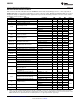
Absolute Maximum Ratings
(1)(2)
V
IN
-0.5V to 7V
FB Voltage -0.5V to 3V
EN Voltage -0.5V to 7V
SW Voltage -0.5V to 7V
ESD Susceptibility Human Body Model
(3)
2 kV
Junction Temperature
(4)
150°C
Storage Temperature −65°C to +150°C
Soldering Information Infrared or Convection Reflow (15 sec) 220°C
(1) Absolute maximum ratings indicate limits beyond which damage to the device may occur. Operating Range indicates conditions for
which the device is intended to be functional, but does not ensure specific performance limits. For ensured specifications and test
conditions, see the Electrical Characteristics.
(2) If Military/Aerospace specified devices are required, please contact the Texas Instruments Sales Office/Distributors for availability and
specifications.
(3) The human body model is a 100pF capacitor discharged through a 1.5 kΩ resistor into each pin. Test method is per JESD-22-A114.
(4) Thermal shutdown will occur if the junction temperature exceeds the maximum junction temperature of the device.
Operating Ratings
V
IN
3V to 5.5V
Junction Temperature −40°C to +125°C
Copyright © 2009–2013, Texas Instruments Incorporated Submit Documentation Feedback 3
Product Folder Links: LM26420