
Datasheet
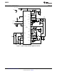

SS/ON1
SS/ON2
LM2642
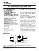
PGOOD1
H
H
L
L
UV_Delay
V
OUT1
1.3V-27V
V
OUT2
1.3V-27V
V
IN
4.5V-30V
LM2642
www.ti.com
SNVS203I –MAY 2002–REVISED APRIL 2013
LM2642 Two-Phase Synchronous Step-Down Switching Controller
Check for Samples: LM2642
1
FEATURES
DESCRIPTION
The LM2642 consists of two current mode
2
• Two Synchronous Buck Regulators
synchronous buck regulator controllers with a
• 180° Out of Phase Operation
switching frequency of 300kHz.
• 4.5V to 30V Input Range
The two switching regulator controllers operate 180°
• Power Good Function Monitors Ch.1
out of phase. This feature reduces the input ripple
• 37µA Shutdown Current
RMS current, thereby significantly reducing the
required input capacitance. The two switching
• 0.04% (typical) Line and Load Regulation Error
regulator outputs can also be paralleled to operate as
• Current Mode Control With or Without a Sense
a dual-phase single output regulator.
Resistor
The output of each channel can be independently
• Independent Enable/Soft-start Pins Allow
adjusted from 1.3 to V
IN
• maximum duty cycle. An
Simple Sequential Startup Configuration.
internal 5V rail is also available externally for driving
• Configurable for Single Output Parallel
bootstrap circuitry.
Operation. (See Figure 3).
Current-mode feedback control assures excellent line
• Adjustable Cycle-by-Cycle Current Limit
and load regulation and a wide loop bandwidth for
• Input Under-voltage Lockout
excellent response to fast load transients. Current is
sensed across either the Vds of the top FET or
• Output Over-voltage Latch Protection
across an external current-sense resistor connected
• Output Under-voltage Protection with Delay
in series with the drain of the top FET. Current limit is
• Thermal Shutdown
independently adjustable for each channel.
• Self Discharge of Output Capacitors When the
The LM2642 features analog soft-start circuitry that is
Regulator is OFF
independent of the output load and output
capacitance. This makes the soft-start behavior more
• TSSOP package
predictable and controllable than traditional soft-start
circuits.
APPLICATIONS
A PGOOD1 pin is provided to monitor the dc output
• Embedded Computer Systems
of channel 1. Over-voltage protection is available for
• High End Gaming Systems
both outputs. A UV-Delay pin is also available to
• Set-top Boxes
allow delayed shut off time for the IC during an output
under-voltage event.
• WebPAD
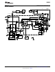
BLOCK DIAGRAM
1
Please be aware that an important notice concerning availability, standard warranty, and use in critical applications of
Texas Instruments semiconductor products and disclaimers thereto appears at the end of this data sheet.
2All trademarks are the property of their respective owners.
PRODUCTION DATA information is current as of publication date.
Copyright © 2002–2013, Texas Instruments Incorporated
Products conform to specifications per the terms of the Texas
Instruments standard warranty. Production processing does not
necessarily include testing of all parameters.