LM26480 www.ti.com SNVS543I – JANUARY 2008 – REVISED MAY 2013 LM26480 Externally Programmable Dual High-Current Step-Down DC/DC and Dual Linear Regulators Check for Samples: LM26480 FEATURES DESCRIPTION • The LM26480 is a multi-functional Power Management Unit, optimized for low-power digital applications. This device integrates two highly efficient 1.5A step-down DC/DC converters and two 300 mA linear regulators. The LM26480 is offered in a tiny 4 x 4 x 0.8mm WQFN-24 pin package.
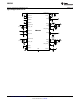
LM26480 SNVS543I – JANUARY 2008 – REVISED MAY 2013 www.ti.com Typical Application Circuit VINLDO12 SYNC 1 µF ENLDO1 nPOR 100k ENLDO2 VIN1 10 µF ENSW1 2.2 µH ENSW2 SW1 VOUTLDO1 0.47 µF R1 C1 R1 C2 R2 10 µF FB1 LDO1_FB R2 GND_SW1 VINLDO1 LM26480 1 µF VIN2 VINLDO2 10 µF 1 µF 2.2 µH VOUTLDO2 SW2 R1 0.
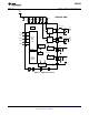
LM26480 www.ti.com SNVS543I – JANUARY 2008 – REVISED MAY 2013 LM26480 PMIC 10 µF 10 µF 19 VIN1 10 1 µF VIN2 24 1 µF VINLDO1 1 1 µF AVDD 1 µF VINLDO2 CVDD 4.7 µF VINLDO12 Input Voltage 13 6 LSW 1 2.2 µH OSC BUCK1 AVDD 2 SYNC VBUCK1 5 SW1 FB1 8 C1 R1 C2 R2 1.2V CSW1 10 µ F 17 ENLDO1 LSW 2 2.2 µH Power ONOFF Logic 16 ENLDO2 7 ENSW1 BUCK2 AVDD VBUCK2 14 SW2 FB2 11 C1 R1 C2 R2 3.
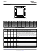
LM26480 SNVS543I – JANUARY 2008 – REVISED MAY 2013 www.ti.com Connection Diagram 18 17 16 15 14 13 19 12 20 11 21 10 22 9 23 8 24 7 1 2 3 4 5 6 Figure 2. 24-Lead WQFN Package (top view) Table 1. Default Options Order Suffix Spec Oscillator Frequency Buck Modes nPOR Delay UVLO Sync AECQ SQ-AA NOPB 2.0 MHz Auto-Mode 60 mS Enabled Disabled No QSQ-AA NOPB 2.0 MHz Auto-Mode 60 mS Enabled Disabled Grade 1 QSQ-CF NOPB 2.
LM26480 www.ti.com SNVS543I – JANUARY 2008 – REVISED MAY 2013 Table 2. PIN DESCRIPTIONS(1) (continued) WQFN Pin No. Name I/O Type Description 14 SW2 O PWR 15 GND_SW2 G G Buck2 NMOS 16 ENLDO2 I D LDO2 enable pin, a logic HIGH enables LDO2. Pin cannot be left floating. 17 ENLDO1 I D LDO1 enable pin, a logic HIGH enables LDO1. Pin cannot be left floating.
LM26480 SNVS543I – JANUARY 2008 – REVISED MAY 2013 Operating Ratings: Bucks www.ti.com (1) (2) (3) VIN 2.8V to 5.5V VEN 0 to (VIN + 0.3V) Junction Temperature (TJ) Range Ambient Temperature (TA) Range (1) (2) (3) (4) –40°C to +125°C (4) −40°C to +85°C Absolute Maximum Ratings indicate limits beyond which damage to the component may occur. Operating Ratings are conditions under which operation of the device is specified. Operating Ratings do not imply ensured performance limits.
LM26480 www.ti.com SNVS543I – JANUARY 2008 – REVISED MAY 2013 General Electrical Characteristics (1) (2) (3) (4) (5) Unless otherwise noted, VIN = 3.6V. Typical values and limits appearing in normal type apply for TJ = 25°C. Limits appearing in boldface type apply over the entire junction temperature range for operation, −40°C to +125°C. Symbol IQ VPOR Parameter Conditions VINLDO12 Shutdown Current VIN = 3.
LM26480 SNVS543I – JANUARY 2008 – REVISED MAY 2013 www.ti.com Buck Converters SW1, SW2 Unless otherwise noted, VIN = 3.6V, CIN = 10 µF, COUT = 10 µF, LOUT = 2.2 µH. Typical values and limits appearing in normal type apply for TJ = 25°C. Limits appearing in boldface type apply over the entire junction temperature range for operation, −40°C to +125°C. ( (1) (2) (3) (4) (5) (6) Symbol VFB (6) Parameter Conditions Min VOUT Units +3 % Line Regulation 0.089 %/V 0.
LM26480 www.ti.com SNVS543I – JANUARY 2008 – REVISED MAY 2013 Typical Performance Characteristics — LDO 2.00 1.50 1.00 0.50 0.00 -0.50 -1.00 -1.50 -2.00 VIN VOUT CHANGE (%) VOUT CHANGE (%) Output Voltage Change vs Temperature (LDO1) VIN = 3.6V, VOUT = 2.5V, 100 mA load Output Voltage Change vs Temperature (LDO2) = 3.6V, VOUT = 1.8V, 100 mA load 2.00 1.50 1.00 0.50 0.00 -0.50 -1.00 -1.50 -2.
LM26480 SNVS543I – JANUARY 2008 – REVISED MAY 2013 www.ti.com Typical Performance Characteristics — LDO (continued) 10 Enable Start-up time (LDO1) 0-3.6 VIN, 2.5 VOUT, 1 mA load Enable Start-up time (LDO2) 0 – 3.6 VIN, 1.8VOUT, 1 mA load Figure 9. Figure 10.
LM26480 www.ti.com SNVS543I – JANUARY 2008 – REVISED MAY 2013 Typical Performance Characteristics — Buck VIN = 2.8V to 5.5V, TA = 25°C Output Voltage vs. Supply Voltage (VOUT = 1.2V) 15 14 13 12 11 10 9 8 7 6 5 4 3 2 1 0 -40 VIN = 5.5V VOUT (V) TEMPERATURE (°C) Shutdown Current vs. Temp VIN = 3.6V VIN = 2.8V -20 0 20 40 60 80 1.250 1.245 1.240 1.235 1.230 1.225 1.220 1.215 1.210 100 LOAD = 1.5A LOAD = 750 mA LOAD = 20 mA 2.5 3.0 3.5 5.0 Figure 12. Output Voltage vs.
LM26480 SNVS543I – JANUARY 2008 – REVISED MAY 2013 www.ti.com Typical Performance Characteristics — Buck Output Current transitions from PFM mode to PWM mode for Buck 1 Efficiency vs. Output Current (VOUT = 1.2V, L = 2.2 µH) Efficiency vs. Output Current (VOUT = 2.0V, L = 2.2 µH) 100 100 VIN = 2.8V EFFICIENCY (%) EFFICIENCY (%) 90 VIN = 3.6V 80 70 VIN = 5.5V 60 50 90 VIN = 2.8V VIN = 3.6V 80 VIN = 5.
LM26480 www.ti.com SNVS543I – JANUARY 2008 – REVISED MAY 2013 Typical Performance Characteristics — Buck VIN= 3.6V, TA = 25°C, VOUT = 1.2V unless otherwise noted Load Transient Response VOUT = 1.2V (PWM Mode) Mode Change by Load Transients VOUT = 1.2V (PWM to PFM) Figure 19. Figure 20. Line Transient Response VIN = 3.6 – 4.2V, VOUT = 1.2V, 250 mA load Line Transient Response VIN = 3.0 – 3.6V, VOUT = 3.0V, 250 mA load Figure 21. Figure 22. Start up into PWM Mode VOUT = 1.2V, 1.
LM26480 SNVS543I – JANUARY 2008 – REVISED MAY 2013 www.ti.com Typical Performance Characteristics — Buck (continued) VIN= 3.6V, TA = 25°C, VOUT = 1.2V unless otherwise noted 14 Start up into PFM Mode VOUT = 1.2V, 30 mA load Start up into PFM Mode VOUT = 3.0V, 30 mA load Figure 25. Figure 26.
LM26480 www.ti.com SNVS543I – JANUARY 2008 – REVISED MAY 2013 DC/DC CONVERTERS Overview The LM26480 provides the DC/DC converters that supply the various power needs of the application by means of two linear low dropout regulators, LDO1 and LDO2, and two buck converters, SW1 and SW2. The table here under lists the output characteristics of the various regulators. Table 3. Supply Specification Output Supply Load LDO1 LDO2 VOUT Range (V) IMAX Maximum Output Current (mA) analog 1.0 to 3.
LM26480 SNVS543I – JANUARY 2008 – REVISED MAY 2013 www.ti.com Circuit Operation Description A buck converter contains a control block, a switching PFET connected between input and output, a synchronous rectifying NFET connected between the output and ground (BCKGND pin) and a feedback path. During the first portion of each switching cycle, the control block turns on the internal PFET switch. This allows current to flow from the input through the inductor to the output filter capacitor and load.
LM26480 www.ti.com SNVS543I – JANUARY 2008 – REVISED MAY 2013 (Typically IMODE < 66 mA + VIN ) 160: (3) During PFM operation, the converter positions the output voltage slightly higher than the nominal output voltage during PWM operation, allowing additional headroom for voltage drop during a load transient from light to heavy load. The PFM comparators sense the output voltage via the feedback pin and control the switching of the output FETs such that the output voltage ramps between 0.8% and 1.
LM26480 SNVS543I – JANUARY 2008 – REVISED MAY 2013 www.ti.com Shutdown Mode During shutdown the PFET switch, reference, control and bias circuitry of the converters are turned off. The NFET switch will be on in shutdown to discharge the output. When the converter is enabled, soft start is activated. It is recommended to disable the converter during the system power up and under voltage conditions when the supply is less than 2.8V.
LM26480 www.ti.com SNVS543I – JANUARY 2008 – REVISED MAY 2013 t1 t2 Case 1 EN1 EN2 RDY1 RDY2 0V Counter delay NPOR t1 t2 Case 2 EN1 EN2 0V RDY1 RDY2 Counter delay NPOR t1 t2 Case 3 EN1 EN2 RDY1 RDY2 Counter delay NPOR Figure 28. NPOR with Counter Delay The above diagram shows the simplest application of the Power-On Reset, where both switcher enables are tied together. In Case 1, EN1 causes nPOR to transition LOW and triggers the nPOR delay counter.
LM26480 SNVS543I – JANUARY 2008 – REVISED MAY 2013 t0 t1 www.ti.com t2 t3 t4 EN1 RDY1 Counter delay NPOR Counter delay EN2 RDY2 Figure 29. Faults Occurring in Counter Delay After Startup The above timing diagram details the Power Good with delay with respect to the enable signals EN1, and EN2. The RDY1, RDY2 are internal signals derived from the output of two comparators.
LM26480 www.ti.com SNVS543I – JANUARY 2008 – REVISED MAY 2013 t0 t1 t2 t3 t4 EN1 RDY1 Counter delay NPOR Case 1: EN2 RDY2 Mask Time Counter delay Mask Window NPOR Case 2: EN2 RDY2 0V Mask Window Mask Time Counter delay NPOR Figure 30. NPOR Mask Window In Case 1, we see that case where EN2 and RDY2 are initiated after triggered programmable delay. To prevent the nPOR being asserted again, a masked window (5 ms) counter delay is triggered off the EN2 rising edge.
LM26480 SNVS543I – JANUARY 2008 – REVISED MAY 2013 www.ti.com Delay Mask Counter EN1 RDY1 EN2 RDY2 S Q R Q NPOR Delay POR Delay Mask Counter Figure 31. Design Implementation of the Flexible Power-On Reset Design implementation of the flexible power-on reset. An internal power-on reset of the IC is used with EN1 and EN2 to produce a reset signal (LOW) to the delay timer nPOR. EN1 and RDY1 or EN2 and RDY2 are used to generate the set signal (HIGH) to the delay timer. S=R=1 never occurs.
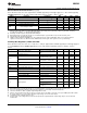
LM26480 www.ti.com SNVS543I – JANUARY 2008 – REVISED MAY 2013 Ideal Resistor Values Target R2 (KΩ) Vout (V) R1 (KΩ) Common R Values R1 (KΩ) R2 (KΩ) Actual VOUT W/ Com/R (V) Actual VOUT Delta from Target (V) Feedback Capacitors C1(pF) C2(pF) 1 200 200 200 200 1 0 15 none ^ 1.1 240 200 240 200 1.1 0 15 none | 1.2 280 200 280 200 1.2 0 12 none | 1.3 320 200 324 200 1.31 0.01 12 none Buck1 1.4 360 200 357 200 1.393 -0.008 10 none And 1.
LM26480 SNVS543I – JANUARY 2008 – REVISED MAY 2013 www.ti.com Inductor Selection for SW1 AND SW2 A nominal inductor value of 2.2 µH is recommended. It is important to ensure the inductor core does not saturate during any foreseeable operational situation. Care should be taken when reviewing the different saturation current ratings that are specified by different manufacturers.
LM26480 www.ti.com SNVS543I – JANUARY 2008 – REVISED MAY 2013 IRIPPLE 8 x F x COUT VCOUT = VROUT = IRIPPLE x ESRCOUT VPPOUT = • • • VCOUT2 + VROUT2 VCOUT: Estimated reactive output ripple VROUT: Estimated real output ripple VPPOUT: Estimated peak-to-peak output ripple (5) The output capacitor needs to be mounted as close as possible to the output pin of the device. For better temperature performance, X7R or X5R types are recommended.
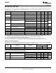
LM26480 SNVS543I – JANUARY 2008 – REVISED MAY 2013 www.ti.com Model Type Vendor Voltage Rating Case Size C2012X5R0J106K Ceramic, X5R TDK 6.3V 0805, (2012) C1608X5R0J106K Ceramic, X5R TDK 6.3V 0603, (1608) Feedback Resistors for LDOs Buck LDO 0.47 µF LM26480 R1 LDO_FB C1 C2 R2 Target VOUT (V) Ideal Resistor Values R1 (KΩ) R2 (KΩ) R1 10 µF Buck_FB R2 Common R Values R1 (KΩ) R2 (KΩ) Actual VOUT W/Com/R (V) 1 200 200 200 200 1 1.1 240 200 240 200 1.1 1.
LM26480 www.ti.com SNVS543I – JANUARY 2008 – REVISED MAY 2013 LDO Dapacitor Selection Input Capacitor An input capacitor is required for stability. It is recommended that a 1.0 μF capacitor be connected between the LDO input pin and ground (this capacitance value may be increased without limit). This capacitor must be located a distance of not more than 1 cm from the input pin and returned to a clean analog ground. Any good quality ceramic, tantalum, or film capacitor may be used at the input.
LM26480 www.ti.com CAP VALUE (% of NOMINAL 1 PF) SNVS543I – JANUARY 2008 – REVISED MAY 2013 0603, 10V, X5R 100% 80% 60% 0402, 6.3V, X5R 40% 20% 0 1.0 2.0 3.0 4.0 5.0 DC BIAS (V) As shown in the graph, increasing the DC bias condition can result in the capacitance value that falls below the minimum value given in the recommended capacitor specifications table. Note that the graph shows the capacitance out of spec for the 0402 case size capacitor at higher bias voltages.
LM26480 www.ti.com SNVS543I – JANUARY 2008 – REVISED MAY 2013 Board Layout Considerations PC board layout is an important part of DC-DC converter design. Poor board layout can disrupt the performance of a DC-DC converter and surrounding circuitry by contributing to EMI, ground bounce, and resistive voltage loss ii the traces. These can send erroneous signals to the DC-DC converter IC, resulting in poor regulation or instability.
LM26480 SNVS543I – JANUARY 2008 – REVISED MAY 2013 www.ti.com High VIN-High Load Operation Additional inforamtion is provided when the IC is operated at extremes of VIN and regulator loads. These are described in terms of the junction temperature and buck output ripple management. Junction Temperature The maximum junction temperature TJ-MAX-OP of 125°C of the IC package.
LM26480 www.ti.com SNVS543I – JANUARY 2008 – REVISED MAY 2013 REVISION HISTORY Changes from Revision H (May 2013) to Revision I • Page Changed layout of National Data Sheet to TI format ..........................................................................................................
PACKAGE OPTION ADDENDUM www.ti.
PACKAGE OPTION ADDENDUM www.ti.com 10-Nov-2013 (3) MSL, Peak Temp. - The Moisture Sensitivity Level rating according to the JEDEC industry standard classifications, and peak solder temperature. (4) There may be additional marking, which relates to the logo, the lot trace code information, or the environmental category on the device. (5) Multiple Device Markings will be inside parentheses. Only one Device Marking contained in parentheses and separated by a "~" will appear on a device.
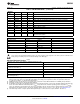
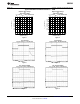
PACKAGE MATERIALS INFORMATION www.ti.com 8-May-2013 TAPE AND REEL INFORMATION *All dimensions are nominal Device Package Package Pins Type Drawing SPQ Reel Reel A0 Diameter Width (mm) (mm) W1 (mm) B0 (mm) K0 (mm) P1 (mm) W Pin1 (mm) Quadrant LM26480QSQ-AA/NOPB WQFN RTW 24 1000 178.0 12.4 4.3 4.3 1.3 8.0 12.0 Q1 LM26480QSQ-CF/NOPB WQFN RTW 24 1000 178.0 12.4 4.3 4.3 1.3 8.0 12.0 Q1 LM26480QSQX-8D/NOPB WQFN RTW 24 4500 330.0 12.4 4.3 4.3 1.3 8.0 12.
PACKAGE MATERIALS INFORMATION www.ti.com 8-May-2013 *All dimensions are nominal Device Package Type Package Drawing Pins SPQ Length (mm) Width (mm) Height (mm) LM26480QSQ-AA/NOPB WQFN RTW 24 1000 210.0 185.0 35.0 LM26480QSQ-CF/NOPB WQFN RTW 24 1000 210.0 185.0 35.0 LM26480QSQX-8D/NOPB WQFN RTW 24 4500 367.0 367.0 35.0 LM26480QSQX-AA/NOPB WQFN RTW 24 4500 367.0 367.0 35.0 LM26480QSQX-CF/NOPB WQFN RTW 24 4500 367.0 367.0 35.
MECHANICAL DATA RTW0024A SQA24A (Rev B) www.ti.
IMPORTANT NOTICE Texas Instruments Incorporated and its subsidiaries (TI) reserve the right to make corrections, enhancements, improvements and other changes to its semiconductor products and services per JESD46, latest issue, and to discontinue any product or service per JESD48, latest issue. Buyers should obtain the latest relevant information before placing orders and should verify that such information is current and complete.