LM2655 LM2655 2.
LM2655 2.5A High Efficiency Synchronous Switching Regulator General Description Features The LM2655 is a current-mode controlled PWM step-down switching regulator. It has the unique ability to operate in synchronous or asynchronous mode. This gives the designer flexibility to choose between the high efficiency of synchronous operation, or the low solution cost of asynchronous operation. Along with flexibility, the LM2655 offers high power density with the small footprint of a TSSOP-16 package.
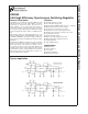
LM2655 Connection Diagram 16-Lead TSSOP (MTC) 10128403 Top View Order Number LM2655MTC-ADJ See NS Package Number MTC16 Block Diagram 10128404 www.national.
LM2655 Pin Description Pin Name Function 1-2 SW Switched-node connection, which is connected to the source of the internal high-side MOSFET. 3-5 PVIN Main power supply input pin. Connected to the drain of the internal high-side MOSFET. 6 VCB Bootstrap capacitor connection for high-side gate drive. 7 AVIN Input voltage for control and drive circuits. 8 SD(SS) Shutdown and Soft-start control pin. Pulling this pin below 0.3V shuts off the regulator.
LM2655 Absolute Maximum Ratings (Note 1) TSSOP-16 Package θJA Power Dissapation If Military/Aerospace specified devices are required, please contact the National Semiconductor Sales Office/ Distributors for availability and specifications. Supply Voltage (PVIN) 3.8V ≤ VIN ≤ 14V Supply Voltage (AVIN) 4.0V ≤ VIN ≤ 14V Feedback Pin Voltage -0.4V ≤ VFB ≤ 5V VCB Voltage, (Note 7) 7V CSS Voltage 2.5V Comp Voltage 2.5V LDELAY Voltage 2.
Specifications with standard typeface are for TJ = 25˚C, and those in boldface type apply over full Operating Temperature Range. VIN = 10V unless otherwise specified. Symbol Parameter Conditions IQ Quiescent Current Shutdown Pin Floating (Device On) Device Not Switching IQSD Quiescent Current in Shutdown Mode Shutdown Pin Pulled Low Switch ON Resistance ISWITCH = 1.
LM2655 All Output Voltage Versions Electrical Characteristics (Continued) Specifications with standard typeface are for TJ = 25˚C, and those in boldface type apply over full Operating Temperature Range. VIN = 10V unless otherwise specified.
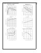
LM2655 Typical Performance Characteristics Efficiency vs VIN (ILOAD = 0.5A) (Synchronous) Efficiency vs Load Current (VIN = 5V, VOUT = 3.3V) 10128405 10128406 lQ vs VIN IQSD vs VIN 10128407 10128408 IQSD vs Junction Temperature Frequency vs Junction Temperature 10128409 10128410 7 www.national.
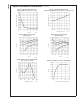
LM2655 Typical Performance Characteristics (Continued) RSW(ON) + Bond Wire Resistance vs Input Voltage (Note 10) (ILOAD = 1.5A) RSW(ON) + Bond Wire Resistance vs Junction Temperature (Note 10) (ILOAD = 1.5A, VIN = 5V ) 10128412 10128411 Current Limit vs Input Voltage (Synchronous) Current Limit vs Input Voltage (Asynchronous) 10128413 10128414 Current Limit vs Junction Temperature (VIN = 5V, VOUT = 3.3V) Reference Voltage vs Junction Temperature 10128415 www.national.
A unique feature of the LM2655 is that it can be operated in either synchronous or asynchronous mode. When operating in asynchronous mode, a small amount of efficiency is sacrificed for a less expensive solution. Any diode may be used, but it is recommended that a low forward drop schottky diode be use to maximize efficiency. When operating the LM2655 in asynchronous mode, the LDR pin should be terminated with a large resistor ( > 1 MegΩ), or left floating.
LM2655 Design Procedure Sprague 593D, 594D, AVX TPS, and CDE polymer aluminum) is recommended. An electrolytic capacitor is not recommended for temperatures below −25˚C since its ESR rises dramatically at cold temperature. A tantalum capacitor has a much better ESR specification at cold temperature and is preferred for low temperature applications.
TSS = CSS * 0.6V/2 µA + CSS * (2V−0.6V)/10 µA (Continued) During start-up, the internal circuit is monitoring the soft-start voltage. When the softstart voltage reaches 2V, the undervoltage and overvoltage protections are enabled. If the output voltage doesn’t rise above 80% of the normal value before the soft-start reaches 2V, undervoltage protection shut down the device. You can avoid this by either increasing the value of the soft-start capacitor, or using a LDELAY capacitor. within 30ns.
LM2655 Design Procedure Application Circuits (Continued) In some applications, the ESR zero Fz1 can not be cancelled by Fp2. Then, Cc2 is needed to introduce Fpc2 to cancel the ESR zero, Fp2 = 1/(2πCc2Ro\Rc). PROGRAMMABLE OUTPUT VOLTAGE The rule of thumb is to have more than 45˚ phase margin at the crossover frequency (G=1). If COUT is higher than 68µF, Cc1 = 2.2nF, and Rc = 15KΩ are good choices for most applications. If the ESR zero is too low to be cancelled by Fp2, add Cc2.
VOUT = (VREF-VADJ)*(RFB1+RFB2)/RFB2 + VADJ where VREF = 1.24V. VADJ can be any voltage higher than VREF (1.24V). In Figure 5, VADJ is produced by an LMV431 adjustable reference following the equation: VADJ = 1.24*(RADJ1/RADJ2 + 1). (Continued) OBTAINING OUTPUT VOLTAGES OF LESS THAN 1.25V Some applications require output voltages less than 1.25V. The circuit shown in Figure 5 will allow the LM2655 to do such a conversion. By referencing the two feedback resistors to VADJ (VADJ > 1.
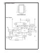
LM2655 10128425 Schematic for the Typical Board Layout Typical PC Board Layout: (2X Size) 10128426 Component Placement Guide 10128427 Component Side PC Board Layout www.national.
LM2655 Typical PC Board Layout: (2X Size) (Continued) 10128428 Solder Side PC Board Layout 15 www.national.
LM2655 2.5A High Efficiency Synchronous Switching Regulator Physical Dimensions inches (millimeters) unless otherwise noted 16-Lead TSSOP (MTC) NS Package Number MTC16 Order Number LM2655MTC-ADJ LM2655MTCX-ADJ LM2655MTC-3.3 LM2655MTCX-3.
IMPORTANT NOTICE Texas Instruments Incorporated and its subsidiaries (TI) reserve the right to make corrections, modifications, enhancements, improvements, and other changes to its products and services at any time and to discontinue any product or service without notice. Customers should obtain the latest relevant information before placing orders and should verify that such information is current and complete.