
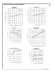
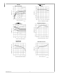
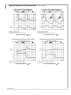
Datasheet
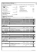

Symbol Parameter Conditions Typ Min Max Units
(Note 4) (Note 5) (Note 5)
V
FB
Feedback Voltage V
IN
= 6.5V to 40V, I
LOAD
= 20 mA to 250 mA
1.210 1.192/1.174 1.228/1.246 V
V
OUT
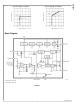
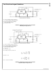
Programmed for 5V
(see Circuit of Figure 3)
η
Efficiency V
IN
= 12V, I
LOAD
= 500 mA 90 %
All Output Voltage Versions
Specifications with standard type face are for T
J
= 25°C, and those in bold type face apply over full Operating Temperature
Range. Unless otherwise specified, V
IN
= 12V for the 3.3V, 5V, and Adjustable versions and V
IN
= 24V for the 12V version, and
I
LOAD
= 100 mA.
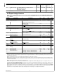
Symbol Parameters Conditions Typ Min Max Units
DEVICE PARAMETERS
I
Q
Quiescent Current V
FEEDBACK
= 8V
2.5
3.6 mA
For 3.3V, 5.0V, and ADJ Versions
V
FEEDBACK
= 15V
2.5
mA
For 12V Versions
I
STBY
Standby Quiescent Current ON/OFF Pin = 0V
50
100/150
μA
I
CL
Current Limit 0.8 0.62/0.575 1.2/1.25 A
I
L
Output Leakage Current V
IN
= 40V, ON/OFF Pin = 0V
1
25
μA
V
SWITCH
= 0V
V
SWITCH
= −1V, ON/OFF Pin = 0V 6 15 mA
R
DS(ON)
Switch On-Resistance I
SWITCH
= 500 mA 0.25 0.40/0.60
Ω
f
O
Oscillator Frequency Measured at Switch Pin 260 225 275 kHz
D Maximum Duty Cycle 95 %
Minimum Duty Cycle 0 %
I
BIAS
Feedback Bias V
FEEDBACK
= 1.3V
85
nA
Current ADJ Version Only
V
S/D
ON/OFF Pin
1.4 0.8 2.0 V
Voltage Thesholds
I
S/D
ON/OFF Pin Current ON/OFF Pin = 0V
20 7 37
μA
F
SYNC
Synchronization Frequency V
SYNC
= 3.5V, 50% duty cycle
400 kHz
V
SYNC
Synchronization Threshold
Voltage
1.4 V
V
SS
Soft-Start Voltage
0.63 0.53 0.73 V
I
SS
Soft-Start Current
4.5 1.5 6.9
μA
θ
JA
Thermal Resistance N Package, Junction to Ambient (Note 6) 95
°C/W
M Package, Junction to Ambient (Note 6) 105
Note 1: Absolute Maximum Ratings indicate limits beyond which damage to the device may occur. Operating Ratings indicate conditions for which the device is
intended to be functional, but device parameter specifications may not be guaranteed under these conditions. For guaranteed specifications and test conditions,
see the Electrical Characteristics.
Note 2: The human body model is a 100 pF capacitor discharged through a 1.5 kΩ resistor into each pin.
Note 3: External components such as the catch diode, inductor, input and output capacitors, and voltage programming resistors can affect switching regulator
performance. When the LM2671 is used as shown in Figure 2 and Figure 3 test circuits, system performance will be as specified by the system parameters section
of the Electrical Characteristics.
Note 4: Typical numbers are at 25°C and represent the most likely norm.
Note 5: All limits guaranteed at room temperature (standard type face) and at temperature extremes (bold type face). All room temperature limits are 100%
production tested. All limits at temperature extremes are guaranteed via correlation using standard Statistical Quality Control (SQC) methods. All limits are used
to calculate Average Outgoing Quality Level (AOQL).
Note 6: Junction to ambient thermal resistance with approximately 1 square inch of printed circuit board copper surrounding the leads. Additional copper area
will lower thermal resistance further. See Application Information section in the application note accompanying this datasheet and the thermal model in LM267X
Made Simple version 6.0 software. The value θ
J−A
for the LLP (LD) package is specifically dependent on PCB trace area, trace material, and the number of layers
and thermal vias. For improved thermal resistance and power dissipation for the LLP package, refer to Application Note AN-1187.
www.national.com 4
LM2671