
Datasheet
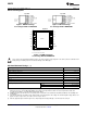

1
2
3
4
7
9
10
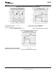
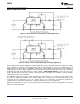
V
SW
CB
*
V
IN
5
6
11
12
13
14
V
SW
GND
ON/OFF
*
*
*
FB
8
V
IN
V
SW
DAP**
*
No Connections
**
Connect to Pin 9 on PCB
*
LM2678
SNVS029I –MARCH 2000–REVISED APRIL 2013
www.ti.com
Connection Diagrams
Top View Top View
Figure 1. DDPAK Package Figure 2. TO-220 Package
See Package Number KTW0007B See Package Number NDZ0007B
Top View
Figure 3. VSON-14 Package
See Package Number NHM0014A
These devices have limited built-in ESD protection. The leads should be shorted together or the device placed in conductive foam
during storage or handling to prevent electrostatic damage to the MOS gates.
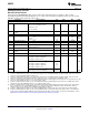
Absolute Maximum Ratings
(1) (2)
Input Supply Voltage 45V
ON/OFF Pin Voltage −0.1V to 6V
Switch Voltage to Ground
(3)
−1V to V
IN
Boost Pin Voltage V
SW
+ 8V
Feedback Pin Voltage −0.3V to 14V
Power Dissipation Internally Limited
ESD
(4)
2 kV
Storage Temperature Range −65°C to 150°C
Soldering Temperature Wave 4 sec, 260°C
Infrared 10 sec, 240°C
Vapor Phase 75 sec, 219°C
(1) Absolute Maximum Ratings are limits beyond which damage to the device may occur. Operating Ratings indicate conditions under
which of the device is ensured. Operating Ratings do not imply ensured performance limits. For ensured performance limits and
associated test condition, see the Electrical Characteristics tables.
(2) If Military/Aerospace specified devices are required, please contact the Texas Instruments Sales Office/Distributors for availability and
specifications.
(3) The absolute maximum specification of the 'Switch Voltage to Ground' applies to DC voltage. An extended negative voltage limit of -10V
applies to a pulse of up to 20 ns, -6V of 60 ns and -3V of up to 100 ns.
(4) ESD was applied using the human-body model, a 100pF capacitor discharged through a 1.5 kΩ resistor into each pin.
2 Submit Documentation Feedback Copyright © 2000–2013, Texas Instruments Incorporated
Product Folder Links: LM2678