
Datasheet
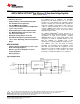

LM2678
SNVS029I –MARCH 2000–REVISED APRIL 2013
www.ti.com
All Output Voltage Versions
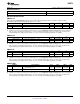
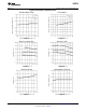
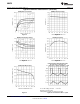
Electrical Characteristics
Limits appearing in bold type face apply over the entire junction temperature range of operation, −40°C to 125°C.
Specifications appearing in normal type apply for T
A
= T
J
= 25°C. Unless otherwise specified V
IN
=12V for the 3.3V, 5V and
Adjustable versions and V
IN
=24V for the 12V version.
Parameter Test Conditions Typ Min Max Units
DEVICE PARAMETERS
I
Q
Quiescent Current V
FEEDBACK
= 8V 4.2 6 mA
For 3.3V, 5.0V, and ADJ Versions
V
FEEDBACK
= 15V
For 12V Versions
I
STBY
Standby Quiescent ON/OFF Pin = 0V
50 100/150 μA
Current
I
CL
Current Limit 7 6.1/5.75 8.3/8.75 A
I
L
Output Leakage Current V
IN
= 40V, ON/OFF Pin = 0V,
μA
V
SWITCH
= 0V, 200
mA
V
SWITCH
= −1V 16 15
R
DS(ON)
Switch On-Resistance I
SWITCH
= 5A 0.12 0.14/0.225 Ω
f
O
Oscillator Frequency Measured at Switch Pin 260 225 280 kHz
D Duty Cycle Maximum Duty Cycle 91 %
Minimum Duty Cycle 0 %
I
BIAS
Feedback Bias Current V
FEEDBACK
= 1.3V ADJ Version Only 85 nA
V
ON/OFF
ON/OFF Threshold
1.4 0.8 2.0 V
Voltage
I
ON/OFF
ON/OFF Input Current ON/OFF Input = 0V 20 45 μA
θ
JA
Thermal Resistance T Package, Junction to Ambient
(1)
65
θ
JA
T Package, Junction to Ambient
(2)
45
θ
JC
T Package, Junction to Case 2
θ
JA
S Package, Junction to Ambient
(3)
56 °C/W
θ
JA
S Package, Junction to Ambient
(4)
35
θ
JA
S Package, Junction to Ambient
(5)
26
θ
JC
S Package, Junction to Case 2 ++
θ
JA
SD Package, Junction to Ambient
(6)
55
°C/W
θ
JA
SD Package, Junction to Ambient
(7)
29
(1) Junction to ambient thermal resistance (no external heat sink) for the 7 lead TO-220 package mounted vertically, with ½ inch leads in a
socket, or on a PC board with minimum copper area.
(2) Junction to ambient thermal resistance (no external heat sink) for the 7 lead TO-220 package mounted vertically, with ½ inch leads
soldered to a PC board containing approximately 4 square inches of (1 oz.) copper area surrounding the leads.
(3) Junction to ambient thermal resistance for the 7 lead DDPAK mounted horizontally against a PC board area of 0.136 square inches (the
same size as the DDPAK package) of 1 oz. (0.0014 in. thick) copper.
(4) Junction to ambient thermal resistance for the 7 lead DDPAK mounted horizontally against a PC board area of 0.4896 square inches
(3.6 times the area of the DDPAK package) of 1 oz. (0.0014 in. thick) copper.
(5) Junction to ambient thermal resistance for the 7 lead DDPAK mounted horizontally against a PC board copper area of 1.0064 square
inches (7.4 times the area of the DDPAK package) of 1 oz. (0.0014 in. thick) copper. Additional copper area will reduce thermal
resistance further. See the thermal model in Switchers Made Simple
®
software.
(6) Junction to ambient thermal resistance for the 14-lead VSON mounted on a PC board copper area equal to the die attach paddle.
(7) Junction to ambient thermal resistance for the 14-lead VSON mounted on a PC board copper area using 12 vias to a second layer of
copper equal to die attach paddle. Additional copper area will reduce thermal resistance further. For layout recommendations, refer to
Application Note AN-1187 at www.ti.com/lsds/ti/analog/powermanagement/power_portal.page.
4 Submit Documentation Feedback Copyright © 2000–2013, Texas Instruments Incorporated
Product Folder Links: LM2678