
Datasheet


LM2695
SNVS413A –JANUARY 2006–REVISED APRIL 2013
www.ti.com
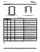
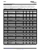
Electrical Characteristics
Specifications with standard type are for T
J
= 25°C only; limits in boldface type apply over the full Operating Junction
Temperature (T
J
) range. Minimum and Maximum limits are ensured through test, design, or statistical correlation. Typical
values represent the most likely parametric norm at T
J
= 25°C, and are provided for reference purposes only. Unless
otherwise stated the following conditions apply: V
IN
= 24V, R
ON
= 200kΩ
(1)
.
Symbol Parameter Conditions Min Typ Max Units
Start-Up Regulator, V
CC
V
CC
Reg V
CC
regulated output 6.6 7 7.4 V
I
CC
= 0 mA, V
V
IN
-V
CC
dropout voltage 1.3
V
CC
= UVLO
VCC
+ 250 mV
V
CC
output impedance 0 mA ≤ I
CC
≤ 5 mA 140 Ω
V
CC
current limit
(2)
V
CC
= 0V 9.7 mA
UVLO
VCC
V
CC
under-voltage lockout V
V
CC
increasing 5.7
threshold
UVLO
VCC
hysteresis V
CC
decreasing 150 mV
UVLO
VCC
filter delay 100 mV overdrive 3 µs
I
IN
operating current Non-switching, FB = 3V 0.5 0.8 mA
I
IN
shutdown current RON/SD = 0V 95 200 µA
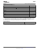
Switch Characteristics
Rds(on) Buck Switch Rds(on) I
TEST
= 200 mA 0.33 0.7 Ω
UVLO
GD
Gate Drive UVLO V
BST
- V
SW
Increasing 3.0 4.4 5.5 V
UVLO
GD
hysteresis 480 mV
Softstart Pin
Pull-up voltage 2.5 V
Internal current source 12.3 µA
Current Limit
I
LIM
Threshold Current out of ISEN 1 1.25 1.5 A
Resistance from ISEN to SGND 130 mΩ
Response time 150 ns
On Timer
t
ON
- 1 On-time V
IN
= 10V, R
ON
= 200 kΩ 2.1 2.8 3.6 µs
t
ON
- 2 On-time V
IN
= 30V, R
ON
= 200 kΩ 950 ns
Shutdown threshold Voltage at RON/SD rising 0.45 0.8 1.2 V
Threshold hysteresis Voltage at RON/SD falling 37 mV
Off Timer
t
OFF
Minimum Off-time 250 ns
Regulation and Over-Voltage Comparators (FB Pin)
V
REF
FB regulation threshold SS pin = steady state 2.440 2.5 2.550 V
FB over-voltage threshold 2.9 V
FB bias current 1 nA
Thermal Shutdown
T
SD
Thermal shutdown temperature 175 °C
Thermal shutdown hysteresis 20 °C
Thermal Resistance
θ
JA
Junction to Ambient °C/W
Both Packages 37
0 LFPM Air Flow
θ
JC
Junction to Case Both Packages 6.6 °C/W
(1) Typical specifications represent the most likely parametric norm at 25°C operation.
(2) V
CC
provides self bias for the internal gate drive and control circuits. Device thermal limitations limit external loading
4 Submit Documentation Feedback Copyright © 2006–2013, Texas Instruments Incorporated
Product Folder Links: LM2695