
Datasheet


FB
SW
L1
C2
R1
R2
V
OUT2
R3
LM2695
LM2695
www.ti.com
SNVS413A –JANUARY 2006–REVISED APRIL 2013
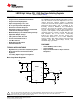
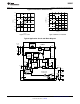
Output voltage regulation is based on ripple voltage at the feedback input, requiring a minimum amount of ESR
for the output capacitor C2. The LM2695 requires a minimum of 25 mV of ripple voltage at the FB pin. In cases
where the capacitor’s ESR is insufficient additional series resistance may be required (R3 in Typical Application
Circuit and Block Diagram).
For applications where lower output voltage ripple is required the output can be taken directly from a low ESR
output capacitor as shown in Figure 5. However, R3 slightly degrades the load regulation.
Figure 5. Low Ripple Output Configuration
Copyright © 2006–2013, Texas Instruments Incorporated Submit Documentation Feedback 7
Product Folder Links: LM2695