
Datasheet
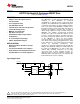


V
CC
LEN
IN
GND
CB
HG
SW
LG
U1
LM27222
1
2
3
4
5
6
7
8
(to controller)
(to controller)
R1
VCC
4V to 6.85V
D1
C2
0.33 PF
C1
Q1
Q2
C3
L1
V
IN
V
OUT
+
C4
+
up to 30V
0.5V to
Vin - 0.5V
LM27222
www.ti.com
SNVS306B –SEPTEMBER 2004–REVISED MARCH 2013
LM27222 High-Speed 4.5A Synchronous MOSFET Driver
Check for Samples: LM27222
1
FEATURES
DESCRIPTION
The LM27222 is a dual N-channel MOSFET driver
2
• Adaptive Shoot-through Protection
designed to drive MOSFETs in push-pull
• 10ns Dead Time
configurations as typically used in synchronous buck
• 8ns Propagation Delay
regulators. The LM27222 takes the PWM output from
a controller and provides the proper timing and drive
• 30ns Minimum On-time
levels to the power stage MOSFETs. Adaptive shoot-
• 0.4Ω Pull-down and 0.9Ω Pull-up Drivers
through protection prevents damaging and efficiency
• 4.5A Peak Driving Current
reducing shoot-through currents, thus ensuring a
robust design capable of being used with nearly any
• MOSFET Tolerant Design
MOSFET. The adaptive shoot-through protection
• 5µA Quiescent Current
circuitry also reduces the dead time down to as low
• 30V Maximum Input Voltage in Buck
as 10ns, ensuring the highest operating efficiency.
Configuration
The peak sourcing and sinking current for each driver
of the LM27222 is about 3A and 4.5Amps
• 4V to 6.85V Operating Voltage
respectively with a Vgs of 5V. System performance is
• SOIC-8 and WSON Packages
also enhanced by keeping propagation delays down
to 8ns. Efficiency is once again improved at all load
APPLICATIONS
currents by supporting synchronous, non-
synchronous, and diode emulation modes through the
• High Current Buck And Boost Voltage
LEN pin. The minimum output pulse width realized at
Converters
the output of the MOSFETs is as low as 30ns. This
• Fast Transient DC/DC Power Supplies
enables high operating frequencies at very high
• Single Ended Forward Output Rectification
conversion ratios in buck regulator designs. To
support low power states in notebook systems, the
• CPU And GPU Core Voltage Regulators
LM27222 draws only 5µA from the 5V rail when the
IN and LEN inputs are low or floating.
Typical Application
1
Please be aware that an important notice concerning availability, standard warranty, and use in critical applications of
Texas Instruments semiconductor products and disclaimers thereto appears at the end of this data sheet.
2All trademarks are the property of their respective owners.
PRODUCTION DATA information is current as of publication date.
Copyright © 2004–2013, Texas Instruments Incorporated
Products conform to specifications per the terms of the Texas
Instruments standard warranty. Production processing does not
necessarily include testing of all parameters.