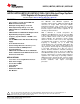
LM27341, LM27342, LM27341-Q1, LM27342-Q1 www.ti.com SNVS497E – NOVEMBER 2008 – REVISED APRIL 2013 LM27341/LM27342/LM27341-Q1/LM27342-Q1 2 MHz 1.5A/2A Wide Input Range Step-Down DC-DC Regulator with Frequency Synchronization Check for Samples: LM27341, LM27342, LM27341-Q1, LM27342-Q1 FEATURES DESCRIPTION • The LM27341 and LM27342 regulators are monolithic, high frequency, PWM step-down DC-DC converters in 10-pin SON and 10-pin MSOPPowerPad packages.
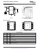
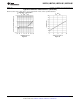
LM27341, LM27342, LM27341-Q1, LM27342-Q1 SNVS497E – NOVEMBER 2008 – REVISED APRIL 2013 www.ti.com Typical Application Circuit VIN PVIN BOOST C2 AVIN L1 C1 VOUT SW C3 D1 LM27341/2 ON EN OFF R1 SYNC CLK FB GND / DAP R2 Figure 1. Figure 2. Efficiency vs Load Current VOUT = 5V, fsw = 2 MHz Connection Diagram SW 1 10 PVIN SW 1 10 PVIN SW 2 9 PVIN SW 2 9 PVIN BOOST 3 8 AVIN BOOST 3 8 AVIN EN 4 7 GND EN 4 7 GND SYNC 5 6 FB SYNC 5 6 FB DAP Figure 3.
LM27341, LM27342, LM27341-Q1, LM27342-Q1 www.ti.com SNVS497E – NOVEMBER 2008 – REVISED APRIL 2013 Absolute Maximum Ratings (1) (2) AVIN, PVIN -0.5V to 24V SW Voltage -0.5V to 24V Boost Voltage -0.5V to 28V Boost to SW Voltage -0.5V to 6.0V FB Voltage -0.5V to 3.0V SYNC Voltage -0.5V to 6.0V EN Voltage -0.5V to (VIN + 0.
LM27341, LM27342, LM27341-Q1, LM27342-Q1 SNVS497E – NOVEMBER 2008 – REVISED APRIL 2013 www.ti.com Electrical Characteristics Specifications with standard typeface are for TJ = 25°C, and those in boldface type apply over the full Operating Temperature Range (TJ = -40°C to 125°C). VIN = 12V, and VBOOST - VSW = 4.3V unless otherwise specified. Datasheet min/max specification limits are ensured by design, test, or statistical analysis. Symbol Parameter Conditions Min Typ Max TJ = 0°C to 85°C 0.990 1.
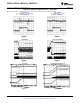
LM27341, LM27342, LM27341-Q1, LM27342-Q1 www.ti.com SNVS497E – NOVEMBER 2008 – REVISED APRIL 2013 Typical Performance Characteristics All curves taken at VIN = 12V, VBOOST - VSW = 4.3V and TA = 25°C, unless specified otherwise. Efficiency vs Load Current VOUT = 5V, fSW = 2 MHz Refer to Figure 40 Load Transient VOUT = 5V, IOUT = 100 mA - 2A @ slewrate = 2A / µs Refer to Figure 40 Figure 5. Figure 6. Efficiency vs Load Current VOUT = 3.3V, fSW = 2 MHz Refer to Figure 46 Load Transient VOUT = 3.
LM27341, LM27342, LM27341-Q1, LM27342-Q1 SNVS497E – NOVEMBER 2008 – REVISED APRIL 2013 www.ti.com Typical Performance Characteristics (continued) All curves taken at VIN = 12V, VBOOST - VSW = 4.3V and TA = 25°C, unless specified otherwise. 6 Line Transient VIN = 10 to 15V, VOUT = 3.3V, no CFF Refer to Figure 49 Line Transient VIN = 10 to 15V, VOUT = 3.3V Refer to Figure 46 Figure 11. Figure 12. Short Circuit Short Circuit Release Figure 13. Figure 14.
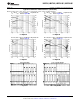
LM27341, LM27342, LM27341-Q1, LM27342-Q1 www.ti.com SNVS497E – NOVEMBER 2008 – REVISED APRIL 2013 Typical Performance Characteristics (continued) All curves taken at VIN = 12V, VBOOST - VSW = 4.3V and TA = 25°C, unless specified otherwise. VIN = 12V, VOUT = 5 V, L = 2.2 µH, COUT = 44 µF Iout =1A Refer to Figure 40 VIN = 12V, VOUT = 3.3V, L = 1.5 µH COUT = 44 µF Iout =1A Refer to Figure 46 Figure 17. Figure 18. VIN = 5V, VOUT = 1.8V, L = 1.
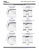
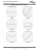
LM27341, LM27342, LM27341-Q1, LM27342-Q1 SNVS497E – NOVEMBER 2008 – REVISED APRIL 2013 www.ti.com Typical Performance Characteristics (continued) All curves taken at VIN = 12V, VBOOST - VSW = 4.3V and TA = 25°C, unless specified otherwise. 8 Oscillator Frequency vs Temperature VSYNC = GND, fSW = 2 MHz Oscillator Frequency vs VFB Figure 23. Figure 24. VFB vs Temperature VFB vs VIN Figure 25. Figure 26. Current Limit vs Temperature VIN = 12V RDSON vs Temperature Figure 27. Figure 28.
LM27341, LM27342, LM27341-Q1, LM27342-Q1 www.ti.com SNVS497E – NOVEMBER 2008 – REVISED APRIL 2013 Typical Performance Characteristics (continued) All curves taken at VIN = 12V, VBOOST - VSW = 4.3V and TA = 25°C, unless specified otherwise. IQ (Shutdown) vs Temperature IQ = IAVIN + IPVIN IEN vs VEN Figure 29. Figure 30.
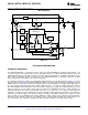
LM27341, LM27342, LM27341-Q1, LM27342-Q1 SNVS497E – NOVEMBER 2008 – REVISED APRIL 2013 www.ti.com Block Diagram BOOST D2 LDO PVIN C2 Switch 0.15: RSENSE L SW VOUT iL + AVIN D1 Driver Current Sense Amplifier C3 EN Under Voltage Lockout PWM Logic Current Limit PWM Comparator Reset Pulse Thermal Shutdown + + + OVP Comparator + ISENSE Error Signal 1.13V Corrective Ramp Soft Start SYNC Oscillator + - FB Internal Compensation + Error Amplifier + VREF +- R1 R2 1.
LM27341, LM27342, LM27341-Q1, LM27342-Q1 www.ti.com SNVS497E – NOVEMBER 2008 – REVISED APRIL 2013 VSW D = tON/TSW SW Voltage VIN tOFF tON 0 -VD1 Inductor Current iL t TSW ILPK IOUT 'iL 0 t Figure 32. LM27341/LM27342 Waveforms of SW Pin Voltage and Inductor Current BOOST FUNCTION Capacitor C2 in Figure 31, commonly referred to as CBOOST, is used to store a voltage VBOOST.
LM27341, LM27342, LM27341-Q1, LM27342-Q1 SNVS497E – NOVEMBER 2008 – REVISED APRIL 2013 www.ti.com D2 VIN PVIN 5V BOOST C2 AVIN L1 C1 VOUT SW C3 D1 LM27342 ON EN OFF R1 SYNC CLK FB GND/DAP R2 Figure 33. External Diode Charges CBOOST HIGH OUTPUT VOLTAGE CONSIDERATIONS When the output voltage is greater than 3.3V, a minimum load current is needed to charge CBOOST, see Figure 34. The minimum load current forward biases the catch diode D1 forcing the SW pin to swing below ground.
LM27341, LM27342, LM27341-Q1, LM27342-Q1 www.ti.com SNVS497E – NOVEMBER 2008 – REVISED APRIL 2013 VIN PVIN BOOST C2 AVIN L1 C1 VOUT SW R3 C3 D1 LM27342 EN R4 R1 SYNC CLK FB GND/DAP R2 Figure 35. Resistor Divider on EN R3 = VIN - 1 x R4 1.8 (6) FREQUENCY SYNCHRONIZATION The LM27341/LM27342 switching frequency can be synchronized to an external clock, between 1.00 and 2.35 MHz, applied at the SYNC pin.
LM27341, LM27342, LM27341-Q1, LM27342-Q1 SNVS497E – NOVEMBER 2008 – REVISED APRIL 2013 www.ti.com OUTPUT OVERVOLTAGE PROTECTION The overvoltage comparator turns off the internal power NFET when the FB pin voltage exceeds the internal reference voltage by 13% (VFB > 1.13 * VREF). With the power NFET turned off the output voltage will decrease toward the regulation level. UNDERVOLTAGE LOCKOUT Undervoltage lockout (UVLO) prevents the LM27341/LM27342 from operating until the input voltage exceeds 2.75V(typ).
LM27341, LM27342, LM27341-Q1, LM27342-Q1 www.ti.com SNVS497E – NOVEMBER 2008 – REVISED APRIL 2013 Figure 36. Recommended Ripple Ratio Vs. Duty Cycle The Duty Cycle (D) can be approximated quickly using the ratio of output voltage (VOUT) to input voltage (VIN): D= VOUT VIN (10) The application's lowest input voltage should be used to calculate the ripple ratio.
LM27341, LM27342, LM27341-Q1, LM27342-Q1 SNVS497E – NOVEMBER 2008 – REVISED APRIL 2013 www.ti.com First the maximum duty cycle is calculated. DMAX = (VOUT + VD1) / (VIN + VD1 - VDS) = (3.3V + 0.5V) / (7V + 0.5V - 0.30V) = 0.528 (14) Using Figure 36 gives us a recommended ripple ratio = 0.4. Now the minimum duty cycle is calculated. DMIN = (VOUT + VD1) / (VIN + VD1 - VDS) = (3.3V + 0.5V) / (16V + 0.5V - 0.30V) = 0.235 (15) The inductance can now be calculated.
LM27341, LM27342, LM27341-Q1, LM27342-Q1 www.ti.com SNVS497E – NOVEMBER 2008 – REVISED APRIL 2013 INPUT CAPACITOR An input capacitor is necessary to ensure that VIN does not drop excessively during switching transients. The primary specifications of the input capacitor are capacitance, voltage, RMS current rating, and Equivalent Series Inductance (ESL). The recommended input capacitance is 10 µF, although 4.7 µF works well for input voltages below 6V.
LM27341, LM27342, LM27341-Q1, LM27342-Q1 SNVS497E – NOVEMBER 2008 – REVISED APRIL 2013 www.ti.com CATCH DIODE The catch diode (D1) conducts during the switch off-time. A Schottky diode is recommended for its fast switching times and low forward voltage drop. The catch diode should be chosen so that its current rating is greater than: ID1 = IOUT x (1-D) (21) The reverse breakdown rating of the diode must be at least the maximum input voltage plus appropriate margin.
LM27341, LM27342, LM27341-Q1, LM27342-Q1 www.ti.com SNVS497E – NOVEMBER 2008 – REVISED APRIL 2013 VDS is the voltage drop across the internal NFET when it is on, and is equal to: VDS = IOUT x RDSON (27) VD is the forward voltage drop across the Schottky diode. It can be obtained from the Electrical Characteristics section of the schottky diode datasheet.
LM27341, LM27342, LM27341-Q1, LM27342-Q1 SNVS497E – NOVEMBER 2008 – REVISED APRIL 2013 www.ti.com TOTAL POWER LOSSES Total power losses are: PLOSS = PCOND + PSWR + PSWF + PQ + PBOOST + PDIODE + PIND (37) Losses internal to the LM27341/LM27342 are: PINTERNAL = PCOND + PSWR + PSWF + PQ + PBOOST (38) EFFICIENCY CALCULATION EXAMPLE Operating conditions are: VIN = 12V VOUT = 3.3V IOUT = 2A fSW = 2 MHz VD1 = 0.5V RDCR = 20 mΩ Internal Power Losses are: PCOND = IOUT2 x RDSON x D = 22 x 0.15Ω x 0.
LM27341, LM27342, LM27341-Q1, LM27342-Q1 www.ti.com SNVS497E – NOVEMBER 2008 – REVISED APRIL 2013 Figure 37. Cross-Sectional View of Integrated Circuit Mounted on a Printed Circuit Board. Heat in the LM27341/LM27342 due to internal power dissipation is removed through conduction and/or convection. Conduction: Heat transfer occurs through cross sectional areas of material.
LM27341, LM27342, LM27341-Q1, LM27342-Q1 SNVS497E – NOVEMBER 2008 – REVISED APRIL 2013 www.ti.com RθJA values for the MSOP-PowerPad @ 1Watt dissipation: Number of Board Layers Size of Bottom Layer Copper Connected to DAP Size of Top Layer Copper Connected to Dap Number of 10 mil Thermal Vias RθJA 2 0.25 in2 0.05 in2 8 80.6 °C/W 2 2 2 0.5625 in 0.05 in 8 70.9 °C/W 2 1 in2 0.05 in2 8 62.1 °C/W 2 1.3225 in2 0.05 in2 8 54.6 °C/W 4 (Eval Board) 3.25 in2 2.25 in2 14 35.
LM27341, LM27342, LM27341-Q1, LM27342-Q1 www.ti.com SNVS497E – NOVEMBER 2008 – REVISED APRIL 2013 METHOD 2 EXAMPLE The operating conditions are the same as the previous Efficiency Calculation: VIN = 12V VOUT = 3.3V IOUT = 2A fSW = 2 MHz VD1 = 0.5V RDCR = 20 mΩ Internal Power Losses are: PCOND = IOUT2 x RDSON x D = 22 x 0.15Ω x 0.314 = 188 mW PSW = (VIN x IOUT x fSW x tFALL) = (12V x 2A x 2 MHz x 10ns) = 480 mW PQ = IQ x VIN = 1.5 mA x 12V = 29 mW PBOOST = IBOOST x VBOOST = 7 mA x 4.
LM27341, LM27342, LM27341-Q1, LM27342-Q1 SNVS497E – NOVEMBER 2008 – REVISED APRIL 2013 www.ti.com METHOD 3 EXAMPLE The operating conditions are the same as the previous Efficiency Calculation: VIN = 12V VOUT = 3.3V IOUT = 2A fSW = 2 MHz VD1 = 0.5V RDCR = 20 mΩ Internal Power Losses are: PCOND = IOUT2 x RDSON x D = 22 x 0.267Ω x .314 = 335 mW PSW = (VIN x IOUT x fSW x tFALL) = (12V x 2A x 2 MHz x 10nS) = 480 mW PQ = IQ x VIN = 1.5 mA x 12V = 29 mW PBOOST = IBOOST x VBOOST = 7 mA x 4.
LM27341, LM27342, LM27341-Q1, LM27342-Q1 www.ti.com SNVS497E – NOVEMBER 2008 – REVISED APRIL 2013 + - Figure 39. Buck Converter Current Loops The dark grey, inner loop represents the high current path during the MOSFET on-time. The light grey, outer loop represents the high current path during the off-time. GROUND PLANE AND SHAPE ROUTING The diagram of Figure 39 is also useful for analyzing the flow of continuous current vs. the flow of pulsating currents.
LM27341, LM27342, LM27341-Q1, LM27342-Q1 SNVS497E – NOVEMBER 2008 – REVISED APRIL 2013 www.ti.com The remaining components should also be placed as close as possible to the IC. Please see Application Note AN-1229 SNVA054 for further considerations and the LM27342 demo board as an example of a four-layer layout.
LM27341, LM27342, LM27341-Q1, LM27342-Q1 www.ti.com SNVS497E – NOVEMBER 2008 – REVISED APRIL 2013 LM27341/LM27342 Circuit Examples VIN PVIN BOOST C2 AVIN L1 C1 VOUT SW C3 D1 LM27341/2 C4 ON EN OFF R1 SYNC CLK 2 MHz FB GND / DAP R2 C5 Figure 40. VIN = 7 - 16V, VOUT = 5V, fSW = 2 MHz, IOUT = Full Load Figure 41. LM27342 Efficiency vs. Load Current Figure 42. Transient Response IOUT = 100 mA - 2A @ slewrate = 2A / µs Table 2.
LM27341, LM27342, LM27341-Q1, LM27342-Q1 SNVS497E – NOVEMBER 2008 – REVISED APRIL 2013 VIN www.ti.com PVIN BOOST C2 AVIN L1 C1 VOUT SW C3 D1 LM27341/2 C4 ON EN OFF R1 SYNC CLK 1 MHz FB GND / DAP R2 C5 Figure 43. VIN = 7 - 16V, VOUT = 5V, fSW = 1 MHz, IOUT = Full Load Figure 44. LM27342 Efficiency vs. Load Current Figure 45. Transient Response IOUT = 100 mA - 2A @ slewrate = 2A / µs Table 3.
LM27341, LM27342, LM27341-Q1, LM27342-Q1 www.ti.com SNVS497E – NOVEMBER 2008 – REVISED APRIL 2013 VIN PVIN BOOST C2 AVIN L1 C1 VOUT SW C3 D1 LM27341/2 C4 ON EN OFF R1 SYNC CLK 2 MHz FB GND / DAP R2 C5 Figure 46. VIN = 5 - 16V, VOUT = 3.3V, fSW = 2 MHz, IOUT = Full Load Figure 47. LM27342 Efficiency vs. Load Current Figure 48. Transient Response IOUT = 100 mA - 2A @ slewrate = 2A / µs Table 4.
LM27341, LM27342, LM27341-Q1, LM27342-Q1 SNVS497E – NOVEMBER 2008 – REVISED APRIL 2013 VIN www.ti.com PVIN BOOST C2 AVIN L1 C1 EN VOUT SW D1 LM27341/2 C3 C4 R1 SYNC FB GND / DAP R2 Figure 49. VIN = 5 - 16V, VOUT = 3.3V, fSW = 2 MHz, IOUT = Full Load Figure 50. LM27342 Efficiency vs. Load Current Figure 51. Transient Response IOUT = 100 mA - 2A @ slewrate = 2A / µs Table 5. Bill of Materials for Figure 49 Part Name Part ID Part Value Part Number Manufacturer Buck Regulator U1 1.
LM27341, LM27342, LM27341-Q1, LM27342-Q1 www.ti.com SNVS497E – NOVEMBER 2008 – REVISED APRIL 2013 VIN PVIN BOOST C2 AVIN L1 C1 VOUT SW D1 LM27341/2 C3 C4 ON EN OFF R1 SYNC CLK 1 MHz FB GND / DAP R2 C5 Figure 52. VIN = 5 - 16V, VOUT = 3.3V, fSW = 1 MHz, IOUT = Full Load Figure 53. LM27342 Efficiency vs. Load Current Figure 54. Transient Response IOUT = 100 mA - 2A @ slewrate = 2A / µs Table 6.
LM27341, LM27342, LM27341-Q1, LM27342-Q1 SNVS497E – NOVEMBER 2008 – REVISED APRIL 2013 VIN www.ti.com PVIN BOOST C2 AVIN L1 C1 EN VOUT SW D1 LM27341/2 C3 C4 R1 SYNC FB GND / DAP R2 Figure 55. VIN = 3.3 - 16V, VOUT = 1.8V, fSW = 2 MHz, IOUT = Full Load Figure 56. LM27342 Efficiency vs. Load Current Figure 57. Transient Response IOUT = 100 mA - 2A @ slewrate = 2A / µs Table 7. Bill of Materials for Figure 55 Part Name Part ID Part Value Part Number Manufacturer Buck Regulator U1 1.
LM27341, LM27342, LM27341-Q1, LM27342-Q1 www.ti.com SNVS497E – NOVEMBER 2008 – REVISED APRIL 2013 VIN PVIN BOOST C2 AVIN L1 C1 VOUT SW D1 LM27341/2 C3 C4 ON EN OFF R1 SYNC CLK 1 MHz FB GND / DAP R2 C5 Figure 58. VIN = 3.3 - 16V, VOUT = 1.8V, fSW = 1 MHz, IOUT = Full Load Figure 59. LM27342 Efficiency vs. Load Current Figure 60. Transient Response IOUT = 100 mA - 2A @ slewrate = 2A / µs Table 8.
LM27341, LM27342, LM27341-Q1, LM27342-Q1 SNVS497E – NOVEMBER 2008 – REVISED APRIL 2013 VIN www.ti.com PVIN BOOST C2 AVIN L1 C1 VOUT SW C3 D1 LM27341/2 C4 ON EN OFF R1 SYNC CLK 2 MHz FB GND / DAP R2 C5 Figure 61. VIN = 3.3 - 9V, VOUT = 1.2V, fSW = 2 MHz, IOUT = Full Load Figure 62. LM27342 Efficiency vs. Load Current Figure 63. Transient Response IOUT = 100 mA - 2A @ slewrate = 2A / µs Table 9.
LM27341, LM27342, LM27341-Q1, LM27342-Q1 www.ti.com SNVS497E – NOVEMBER 2008 – REVISED APRIL 2013 REVISION HISTORY Changes from Revision D (April 2013) to Revision E • Page Changed layout of National Data Sheet to TI format ..........................................................................................................
PACKAGE OPTION ADDENDUM www.ti.
PACKAGE OPTION ADDENDUM www.ti.com 11-Apr-2013 Pb-Free (RoHS): TI's terms "Lead-Free" or "Pb-Free" mean semiconductor products that are compatible with the current RoHS requirements for all 6 substances, including the requirement that lead not exceed 0.1% by weight in homogeneous materials. Where designed to be soldered at high temperatures, TI Pb-Free products are suitable for use in specified lead-free processes.
PACKAGE MATERIALS INFORMATION www.ti.com 8-Apr-2013 TAPE AND REEL INFORMATION *All dimensions are nominal Device Package Package Pins Type Drawing SPQ Reel Reel A0 Diameter Width (mm) (mm) W1 (mm) B0 (mm) K0 (mm) P1 (mm) W Pin1 (mm) Quadrant LM27341MY/NOPB MSOPPower PAD DGQ 10 1000 178.0 12.4 5.3 3.4 1.4 8.0 12.0 Q1 LM27341MYX/NOPB MSOPPower PAD DGQ 10 3500 330.0 12.4 5.3 3.4 1.4 8.0 12.0 Q1 LM27341QMY/NOPB MSOPPower PAD DGQ 10 1000 178.0 12.4 5.3 3.4 1.4 8.
PACKAGE MATERIALS INFORMATION www.ti.com 8-Apr-2013 Device Package Package Pins Type Drawing SPQ Reel Reel A0 Diameter Width (mm) (mm) W1 (mm) B0 (mm) K0 (mm) P1 (mm) W Pin1 (mm) Quadrant PAD LM27342QMYX/NOPB MSOPPower PAD DGQ 10 3500 330.0 12.4 5.3 3.4 1.4 8.0 12.0 Q1 LM27342SD/NOPB WSON DSC 10 1000 178.0 12.4 3.3 3.3 1.0 8.0 12.0 Q1 LM27342SDX/NOPB WSON DSC 10 4500 330.0 12.4 3.3 3.3 1.0 8.0 12.
PACKAGE MATERIALS INFORMATION www.ti.com 8-Apr-2013 Device Package Type Package Drawing Pins SPQ Length (mm) Width (mm) Height (mm) LM27342SDX/NOPB WSON DSC 10 4500 367.0 367.0 35.
MECHANICAL DATA DGQ0010A MUC10A (Rev A) BOTTOM VIEW www.ti.
MECHANICAL DATA DSC0010A SDA10A (Rev A) www.ti.
IMPORTANT NOTICE Texas Instruments Incorporated and its subsidiaries (TI) reserve the right to make corrections, enhancements, improvements and other changes to its semiconductor products and services per JESD46, latest issue, and to discontinue any product or service per JESD48, latest issue. Buyers should obtain the latest relevant information before placing orders and should verify that such information is current and complete.