
Datasheet
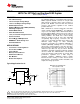
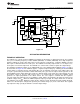
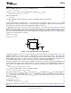

V
IN
V
IN
EN
BOOST
SW
FB
GND
V
OUT
C3
L1
C1
C2
R1
R2
D1
D2
ON
OFF
LM2736
www.ti.com
SNVS316F –SEPTEMBER 2004–REVISED APRIL 2013
LM2736 Thin SOT 750mA Load Step-Down DC-DC Regulator
Check for Samples: LM2736
1
FEATURES
DESCRIPTION
The LM2736 regulator is a monolithic, high frequency,
23
• Thin SOT-6 Package
PWM step-down DC/DC converter in a 6-pin Thin
• 3.0V to 18V Input Voltage Range
SOT package. It provides all the active functions to
• 1.25V to 16V Output Voltage Range
provide local DC/DC conversion with fast transient
response and accurate regulation in the smallest
• 750mA Output Current
possible PCB area.
• 550kHz (LM2736Y) and 1.6MHz (LM2736X)
With a minimum of external components and online
Switching Frequencies
design support through WEBENCH
®
, the LM2736 is
• 350mΩ NMOS Switch
easy to use. The ability to drive 750mA loads with an
• 30nA Shutdown Current
internal 350mΩ NMOS switch using state-of-the-art
• 1.25V, 2% Internal Voltage Reference
0.5µm BiCMOS technology results in the best power
density available. The world class control circuitry
• Internal Soft-Start
allows for on-times as low as 13ns, thus supporting
• Current-Mode, PWM Operation
exceptionally high frequency conversion over the
• WEBENCH
®
Online Design Tool
entire 3V to 18V input operating range down to the
minimum output voltage of 1.25V. Switching
• Thermal Shutdown
frequency is internally set to 550kHz (LM2736Y) or
1.6MHz (LM2736X), allowing the use of extremely
APPLICATIONS
small surface mount inductors and chip capacitors.
• Local Point of Load Regulation
Even though the operating frequencies are very high,
efficiencies up to 90% are easy to achieve. External
• Core Power in HDDs
shutdown is included, featuring an ultra-low stand-by
• Set-Top Boxes
current of 30nA. The LM2736 utilizes current-mode
• Battery Powered Devices
control and internal compensation to provide high-
performance regulation over a wide range of
• USB Powered Devices
operating conditions. Additional features include
• DSL Modems
internal soft-start circuitry to reduce inrush current,
• Notebook Computers
pulse-by-pulse current limit, thermal shutdown, and
output over-voltage protection.
Typical Application Circuit
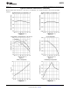
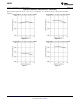
Efficiency vs Load Current "X"
V
IN
= 5V, V
OUT
= 3.3V
1
Please be aware that an important notice concerning availability, standard warranty, and use in critical applications of
Texas Instruments semiconductor products and disclaimers thereto appears at the end of this data sheet.
2WEBENCH is a registered trademark of Texas Instruments.
3All other trademarks are the property of their respective owners.
PRODUCTION DATA information is current as of publication date.
Copyright © 2004–2013, Texas Instruments Incorporated
Products conform to specifications per the terms of the Texas
Instruments standard warranty. Production processing does not
necessarily include testing of all parameters.