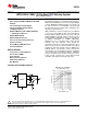
LM2738 www.ti.com SNVS556B – APRIL 2008 – REVISED APRIL 2013 LM2738 550kHz/1.6MHz 1.5A Step-Down DC-DC Switching Regulator Check for Samples: LM2738 FEATURES DESCRIPTION • The LM2738 regulator is a monolithic, high frequency, PWM step-down DC/DC converter in an 8-pin WSON or 8-pin MSOP-PowerPAD package. It provides all the active functions for local DC/DC conversion with fast transient response and accurate regulation in the smallest possible PCB area.
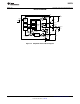
LM2738 SNVS556B – APRIL 2008 – REVISED APRIL 2013 www.ti.com Connection Diagrams Figure 1. 8-Pin WSON (Top View) See Package Number NGQ Figure 2. 8-Pin MSOP-PowerPAD (Top View) See Package Number DGN PIN DESCRIPTIONS Pin Name 1 BOOST 2 VIN Supply voltage for output power stage. Connect a bypass capacitor to this pin. Must tie pins 2 and 3 together at package. 3 VCC Input supply voltage of the IC. Connect a bypass capacitor to this pin. Must tie pin 2 and 3 together at the package.
LM2738 www.ti.com SNVS556B – APRIL 2008 – REVISED APRIL 2013 ABSOLUTE MAXIMUM RATINGS (1) (2) VIN, VCC -0.5V to 24V SW Voltage -0.5V to 24V Boost Voltage -0.5V to 30V Boost to SW Voltage -0.5V to 6.0V FB Voltage -0.5V to 3.0V EN Voltage -0.5V to (VIN + 0.3V) Junction Temperature ESD Susceptibility 150°C (3) 2kV Storage Temp. Range Soldering Information (1) (2) (3) -65°C to 150°C Infrared/Convection Reflow (15sec) 220°C Wave Soldering Lead Temp.
LM2738 SNVS556B – APRIL 2008 – REVISED APRIL 2013 www.ti.com ELECTRICAL CHARACTERISTICS Specifications with standard typeface are for TJ = 25°C, and those in boldface type apply over the full Operating Temperature Range (TJ = -40°C to 125°C). VIN = 12V, VBOOST - VSW = 5V unless otherwise specified. Datasheet min/max specification limits are ensured by design, test, or statistical analysis. Symbol VFB ΔVFB/ΔVIN IFB UVLO Parameter Conditions Feedback Voltage Min (1) Typ (2) Max (1) 0.784 0.800 0.
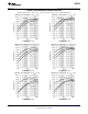
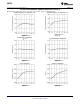
LM2738 www.ti.com SNVS556B – APRIL 2008 – REVISED APRIL 2013 TYPICAL PERFORMANCE CHARACTERISTICS All curves taken at VIN = 12V, VBOOST - VSW = 5V, and TA = 25°C, unless specified otherwise. Efficiency vs Load Current - "X" VOUT = 5V Efficiency vs Load Current - "Y" VOUT = 5V Figure 3. Figure 4. Efficiency vs Load Current - "X" VOUT = 3.3V Efficiency vs Load Current - "Y" VOUT = 3.3V Figure 5. Figure 6. Efficiency vs Load Current - "X" VOUT = 1.5V Efficiency vs Load Current - "Y" VOUT = 1.
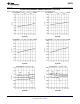
LM2738 SNVS556B – APRIL 2008 – REVISED APRIL 2013 www.ti.com TYPICAL PERFORMANCE CHARACTERISTICS (continued) All curves taken at VIN = 12V, VBOOST - VSW = 5V, and TA = 25°C, unless specified otherwise. 6 Oscillator Frequency vs Temperature - "X" Oscillator Frequency vs Temperature - "Y" Figure 9. Figure 10. Current Limit vs Temperature VIN = 5V IQ Non-Switching vs Temperature Figure 11. Figure 12. VFB vs Temperature RDSON vs Temperature Figure 13. Figure 14.
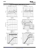
LM2738 www.ti.com SNVS556B – APRIL 2008 – REVISED APRIL 2013 TYPICAL PERFORMANCE CHARACTERISTICS (continued) All curves taken at VIN = 12V, VBOOST - VSW = 5V, and TA = 25°C, unless specified otherwise. Line Regulation - "X" (VOUT = 1.5V, IOUT = 750mA) Line Regulation - "Y" (VOUT = 1.5V, IOUT = 750mA) Figure 15. Figure 16. Line Regulation - "X" (VOUT = 3.3V, IOUT = 750mA) Line Regulation - "Y" (VOUT = 3.3V, IOUT = 750mA) Figure 17. Figure 18. Load Regulation - "X" (VOUT = 1.
LM2738 SNVS556B – APRIL 2008 – REVISED APRIL 2013 www.ti.com TYPICAL PERFORMANCE CHARACTERISTICS (continued) All curves taken at VIN = 12V, VBOOST - VSW = 5V, and TA = 25°C, unless specified otherwise. 8 Load Regulation - "X" (VOUT = 3.3V) Load Regulation - "Y" (VOUT = 3.3V) Figure 21. Figure 22. IQ Switching vs Temperature Load Transient - "X" (VOUT = 3.3V, VIN = 12V) Figure 23. Figure 24. Startup - "X" (VOUT = 3.3V, VIN = 12, IOUT=1.5A (Resistive Load)) In-Rush Current - "X" (VOUT = 3.
LM2738 www.ti.com SNVS556B – APRIL 2008 – REVISED APRIL 2013 BLOCK DIAGRAM VIN VIN Current-Sense Amplifier OFF EN CIN D2 Thermal Shutdown BOOST VBOOST Under Voltage Lockout Oscillator RSENSE + - Current Limit Output Control Logic Reset Pulse + ISENSE + + Corrective Ramp 0.25: Switch Driver SW OVP Comparator - ON Internal Regulator and Enable Circuit Error Signal D1 + PWM Comparator CBOOST VSW L IL VOUT COUT 0.
LM2738 SNVS556B – APRIL 2008 – REVISED APRIL 2013 www.ti.com APPLICATION INFORMATION THEORY OF OPERATION The LM2738 is a constant frequency PWM buck regulator IC that delivers a 1.5A load current. The regulator has a preset switching frequency of either 550kHz (LM2738Y) or 1.6MHz (LM2738X). These high frequencies allow the LM2738 to operate with small surface mount capacitors and inductors, resulting in DC/DC converters that require a minimum amount of board space.
LM2738 www.ti.com SNVS556B – APRIL 2008 – REVISED APRIL 2013 BOOST FUNCTION Capacitor CBOOST and diode D2 in Figure 29 are used to generate a voltage VBOOST. VBOOST - VSW is the gate drive voltage to the internal NMOS control switch. To properly drive the internal NMOS switch during its on-time, VBOOST needs to be at least 2.5V greater than VSW. It is recommended that VBOOST be greater than 2.5V above VSW for best efficiency. VBOOST – VSW should not exceed the maximum operating limit of 5.5V. 5.
LM2738 SNVS556B – APRIL 2008 – REVISED APRIL 2013 www.ti.com D2 D3 VIN BOOST VIN VBOOST CBOOST LM2738 CIN L VOUT SW GND COUT D1 Figure 30. Zener Reduces Boost Voltage from VIN An alternative method is to place the zener diode D3 in a shunt configuration as shown in Figure 31. A small 350mW to 500mW 5.1V zener in a SOT-23 or SOD package can be used for this purpose. A small ceramic capacitor such as a 6.3V, 0.1µF capacitor (C4) should be placed in parallel with the zener diode.
LM2738 www.ti.com SNVS556B – APRIL 2008 – REVISED APRIL 2013 For example, using the X-version let VIN = 10V, VZENER = 5V, VD2 = 0.7V, IZENER = 1mA, and duty cycle D = 50%. Then IBOOST = 0.56 x (0.5 + 0.54) x (5 - 0.7) mA = 2.5mA R3 = (10V - 5V) / (1.4 x 2.5mA + 1mA) = 1.11kΩ (10) (11) ENABLE PIN / SHUTDOWN MODE The LM2738 has a shutdown mode that is controlled by the enable pin (EN).
LM2738 SNVS556B – APRIL 2008 – REVISED APRIL 2013 www.ti.com Design Guide INDUCTOR SELECTION The Duty Cycle (D) can be approximated quickly using the ratio of output voltage (VO) to input voltage (VIN): VO D= VIN (12) The catch diode (D1) forward voltage drop and the voltage drop across the internal NMOS switch must be included to calculate a more accurate duty cycle.
LM2738 www.ti.com SNVS556B – APRIL 2008 – REVISED APRIL 2013 When selecting an inductor, make sure that it is capable of supporting the peak output current without saturating. Inductor saturation will result in a sudden reduction in inductance and prevent the regulator from operating correctly. Because of the speed of the internal current limit, the peak current of the inductor need only be specified for the required maximum output current. For example, if the designed maximum output current is 1.
LM2738 SNVS556B – APRIL 2008 – REVISED APRIL 2013 www.ti.com CATCH DIODE The catch diode (D1) conducts during the switch off-time. A Schottky diode is recommended for its fast switching times and low forward voltage drop. The catch diode should be chosen so that its current rating is greater than: ID1 = IOUT x (1-D) (23) The reverse breakdown rating of the diode must be at least the maximum input voltage plus appropriate margin.
LM2738 www.ti.com SNVS556B – APRIL 2008 – REVISED APRIL 2013 Calculating Efficiency, and Junction Temperature The complete LM2738 DC/DC converter efficiency can be calculated in the following manner. (26) Or (27) Calculations for determining the most significant power losses are shown below. Other losses totaling less than 2% are not discussed. Power loss (PLOSS) is the sum of two basic types of losses in the converter: switching and conduction.
LM2738 SNVS556B – APRIL 2008 – REVISED APRIL 2013 www.ti.com Another significant external power loss is the conduction loss in the output inductor. The equation can be simplified to: PIND = IOUT2 x RDCR (32) The LM2738 conduction loss is mainly associated with the internal NFET switch: (33) If the inductor ripple current is fairly small, the conduction losses can be simplified to: PCOND = IOUT2 x RDSON x D (34) Switching losses are also associated with the internal NFET switch.
LM2738 www.ti.com SNVS556B – APRIL 2008 – REVISED APRIL 2013 Heat in the LM2738 due to internal power dissipation is removed through conduction and/or convection. Conduction: Heat transfer occurs through cross sectional areas of material. Depending on the material, the transfer of heat can be considered to have poor to good thermal conductivity properties (insulator vs. conductor). Heat Transfer goes as: Silicon → package → lead frame → PCB Convection: Heat transfer is by means of airflow.
LM2738 SNVS556B – APRIL 2008 – REVISED APRIL 2013 www.ti.com The second method can give a very accurate silicon junction temperature. The first step is to determine RθJA of the application. The LM2738 has over-temperature protection circuitry. When the silicon temperature reaches 165°C, the device stops switching. The protection circuitry has a hysteresis of about 15°C. Once the silicon temperature has decreased to approximately 150°C, the device will start to switch again.
LM2738 www.ti.com SNVS556B – APRIL 2008 – REVISED APRIL 2013 Figure 35. 8-Lead WSON PCB Dog Bone Layout LM2738X Circuit Example 1 D2 VIN BOOST VIN C3 C1 R3 L1 SW LM2738 ON VOUT D1 EN OFF C2 R1 FB GND R2 Figure 36. LM2738X (1.6MHz) VBOOST Derived from VIN 5V to 1.5V/1.5A Table 2. Bill of Materials for Figure 36 Part ID Part Value Part Number Manufacturer U1 1.5A Buck Regulator LM2738X Texas Instruments C1, Input Cap 10µF, 6.3V, X5R C3216X5ROJ106M TDK C2, Output Cap 22µF, 6.
LM2738 SNVS556B – APRIL 2008 – REVISED APRIL 2013 www.ti.com LM2738X Circuit Example 2 Figure 37. LM2738X (1.6MHz) VBOOST Derived from VOUT 12V to 3.3V/1.5A Table 3. Bill of Materials for Figure 37 Part ID Part Value Part Number Manufacturer U1 1.5A Buck Regulator LM2738X Texas Instruments C1, Input Cap 10µF, 25V, X7R C3225X7R1E106M TDK C2, Output Cap 33µF, 6.3V, X5R C3216X5ROJ336M TDK C3, Boost Cap 0.1µF, 16V, X7R C1005X7R1C104K TDK D1, Catch Diode 0.34VF Schottky 1.
LM2738 www.ti.com SNVS556B – APRIL 2008 – REVISED APRIL 2013 LM2738X Circuit Example 3 C4 D3 R4 D2 BOOST VIN VIN C3 C1 R3 L1 SW VOUT LM2738 ON D1 EN OFF C2 R1 FB GND R2 Figure 38. LM2738X (1.6MHz) VBOOST Derived from VSHUNT 18V to 1.5V/1.5A Table 4. Bill of Materials for Figure 38 Part ID Part Value Part Number Manufacturer U1 1.5A Buck Regulator LM2738X Texas Instruments C1, Input Cap 10µF, 25V, X7R C3225X7R1E106M TDK C2, Output Cap 47µF, 6.
LM2738 SNVS556B – APRIL 2008 – REVISED APRIL 2013 www.ti.com LM2738X Circuit Example 4 D3 D2 BOOST VIN VIN C1 C3 R3 LM2738 ON VOUT D1 EN OFF L1 SW C2 R1 FB GND R2 Figure 39. LM2738X (1.6MHz) VBOOST Derived from Series Zener Diode (VIN) 15V to 1.5V/1.5A Table 5. Bill of Materials for Figure 39 Part ID Part Value Part Number Manufacturer U1 1.5A Buck Regulator LM2738X Texas Instruments C1, Input Cap 10µF, 25V, X7R C3225X7R1E106M TDK C2, Output Cap 47µF, 6.
LM2738 www.ti.com SNVS556B – APRIL 2008 – REVISED APRIL 2013 LM2738X Circuit Example 5 D3 D2 VIN BOOST VIN C3 C1 R3 LM2738 ON VOUT D1 EN OFF L1 SW C2 R1 FB GND R2 Figure 40. LM2738X (1.6MHz) VBOOST Derived from Series Zener Diode (VOUT) 15V to 9V/1.5A Table 6. Bill of Materials for Figure 40 Part ID Part Value Part Number Manufacturer U1 1.
LM2738 SNVS556B – APRIL 2008 – REVISED APRIL 2013 www.ti.com LM2738Y Circuit Example 6 D2 VIN BOOST VIN C3 C1 R3 L1 SW LM2738 ON VOUT D1 EN OFF C2 R1 FB GND R2 Figure 41. LM2738Y (550kHz) VBOOST Derived from VIN 5V to 1.5V/1.5A Table 7. Bill of Materials for Figure 41 Part ID Part Value Part Number Manufacturer U1 1.5A Buck Regulator LM2738Y Texas Instruments C1, Input Cap 10µF, 6.3V, X5R C3216X5ROJ106M TDK C2, Output Cap 47µF, 6.3V, X5R C3216X5ROJ476M TDK C3, Boost Cap 0.
LM2738 www.ti.com SNVS556B – APRIL 2008 – REVISED APRIL 2013 LM2738Y Circuit Example 7 Figure 42. LM2738Y (550kHz) VBOOST Derived from VOUT 12V to 3.3V/1.5A Table 8. Bill of Materials for Figure 42 Part ID Part Value Part Number Manufacturer U1 1.5A Buck Regulator LM2738Y Texas Instruments C1, Input Cap 10µF, 25V, X7R C3225X7R1E106M TDK C2, Output Cap 47µF, 6.3V, X5R C3216X5ROJ476M TDK C3, Boost Cap 0.1µF, 16V, X7R C1005X7R1C104K TDK D1, Catch Diode 0.34VF Schottky 1.
LM2738 SNVS556B – APRIL 2008 – REVISED APRIL 2013 www.ti.com LM2738Y Circuit Example 8 C4 D3 R4 D2 BOOST VIN VIN C3 C1 R3 L1 SW VOUT LM2738 ON D1 EN OFF C2 R1 FB GND R2 Figure 43. LM2738Y (550kHz) VBOOST Derived from VSHUNT 18V to 1.5V/1.5A Table 9. Bill of Materials for Figure 43 Part ID Part Value Part Number Manufacturer U1 1.5A Buck Regulator LM2738Y Texas Instruments C1, Input Cap 10µF, 25V, X7R C3225X7R1E106M TDK C2, Output Cap (47µF, 6.
LM2738 www.ti.com SNVS556B – APRIL 2008 – REVISED APRIL 2013 LM2738Y Circuit Example 9 D3 D2 BOOST VIN VIN C1 C3 R3 LM2738 ON VOUT D1 EN OFF L1 SW C2 R1 FB GND R2 Figure 44. LM2738Y (550kHz) VBOOST Derived from Series Zener Diode (VIN) 15V to 1.5V/1.5A Table 10. Bill of Materials for Figure 44 Part ID Part Value Part Number Manufacturer U1 1.5A Buck Regulator LM2738Y Texas Instruments C1, Input Cap 10µF, 25V, X7R C3225X7R1E106M TDK C2, Output Cap (47µF, 6.
LM2738 SNVS556B – APRIL 2008 – REVISED APRIL 2013 www.ti.com LM2738Y Circuit Example 10 D3 D2 VIN BOOST VIN C3 C1 R3 LM2738 ON VOUT D1 EN OFF L1 SW C2 R1 FB GND R2 Figure 45. LM2738Y (550kHz) VBOOST Derived from Series Zener Diode (VOUT) 15V to 9V/1.5A Table 11. Bill of Materials for Figure 45 Part ID Part Value Part Number Manufacturer U1 1.
LM2738 www.ti.com SNVS556B – APRIL 2008 – REVISED APRIL 2013 REVISION HISTORY Changes from Revision A (April 2013) to Revision B • Page Changed layout of National Data Sheet to TI format ..........................................................................................................
PACKAGE OPTION ADDENDUM www.ti.
PACKAGE OPTION ADDENDUM www.ti.com 11-Apr-2013 (4) Multiple Top-Side Markings will be inside parentheses. Only one Top-Side Marking contained in parentheses and separated by a "~" will appear on a device. If a line is indented then it is a continuation of the previous line and the two combined represent the entire Top-Side Marking for that device. Important Information and Disclaimer:The information provided on this page represents TI's knowledge and belief as of the date that it is provided.
PACKAGE MATERIALS INFORMATION www.ti.com 23-Oct-2013 TAPE AND REEL INFORMATION *All dimensions are nominal Device Package Package Pins Type Drawing SPQ Reel Reel A0 Diameter Width (mm) (mm) W1 (mm) B0 (mm) K0 (mm) P1 (mm) W Pin1 (mm) Quadrant LM2738XMY/NOPB MSOPPower PAD DGN 8 1000 178.0 12.4 5.3 3.4 1.4 8.0 12.0 Q1 LM2738XMYX/NOPB MSOPPower PAD DGN 8 3500 330.0 12.4 5.3 3.4 1.4 8.0 12.0 Q1 LM2738XSD/NOPB WSON NGQ 8 1000 178.0 12.4 3.3 3.3 1.0 8.0 12.
PACKAGE MATERIALS INFORMATION www.ti.com 23-Oct-2013 *All dimensions are nominal Device Package Type Package Drawing Pins SPQ Length (mm) Width (mm) Height (mm) LM2738XMY/NOPB MSOP-PowerPAD DGN 8 1000 210.0 185.0 35.0 LM2738XMYX/NOPB MSOP-PowerPAD DGN 8 3500 367.0 367.0 35.0 LM2738XSD/NOPB WSON NGQ 8 1000 213.0 191.0 55.0 LM2738XSDX/NOPB WSON NGQ 8 4500 367.0 367.0 35.0 LM2738YMY/NOPB MSOP-PowerPAD DGN 8 1000 210.0 185.0 35.
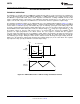
MECHANICAL DATA DGN0008A MUY08A (Rev A) BOTTOM VIEW www.ti.
MECHANICAL DATA NGQ0008A SDA08A (Rev A) www.ti.
IMPORTANT NOTICE Texas Instruments Incorporated and its subsidiaries (TI) reserve the right to make corrections, enhancements, improvements and other changes to its semiconductor products and services per JESD46, latest issue, and to discontinue any product or service per JESD48, latest issue. Buyers should obtain the latest relevant information before placing orders and should verify that such information is current and complete.