
Datasheet
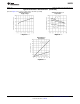


1
2
3
6
5
4
LM2766
www.ti.com
SNVS071B –MARCH 2000–REVISED MAY 2013
LM2766 Switched Capacitor Voltage Converter
Check for Samples: LM2766
1
FEATURES
DESCRIPTION
The LM2766 CMOS charge-pump voltage converter
2
• Doubles Input Supply Voltage
operates as a voltage doubler for an input voltage in
• SOT-23 6-Pin Package
the range of +1.8V to +5.5V. Two low cost capacitors
• 20Ω Typical Output Impedance
and a diode are used in this circuit to provide up to 20
mA of output current.
• 90% Typical Conversion Efficiency at 20 mA
• 0.1µA Typical Shutdown Current
The LM2766 operates at 200 kHz switching
frequency to reduce output resistance and voltage
ripple. With an operating current of only 350 µA
APPLICATIONS
(operating efficiency greater than 90% with most
• Cellular Phones
loads) and 0.1µA typical shutdown current, the
• Pagers
LM2766 provides ideal performance for battery
powered systems. The device is manufactured in a
• PDAs
SOT-23 6-pin package.
• Operational Amplifier Power Supplies
• Interface Power Supplies
• Handheld Instruments
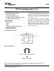
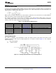
Basic Application Circuits
Figure 1. Voltage Doubler
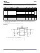
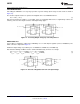
Connection Diagram
Figure 2. DBV Package Top View
Figure 3. Actual Size
1
Please be aware that an important notice concerning availability, standard warranty, and use in critical applications of
Texas Instruments semiconductor products and disclaimers thereto appears at the end of this data sheet.
2All trademarks are the property of their respective owners.
PRODUCTION DATA information is current as of publication date.
Copyright © 2000–2013, Texas Instruments Incorporated
Products conform to specifications per the terms of the Texas
Instruments standard warranty. Production processing does not
necessarily include testing of all parameters.