
Datasheet

LM2931-N
SNOSBE5G –MARCH 2000–REVISED APRIL 2013
www.ti.com
These devices have limited built-in ESD protection. The leads should be shorted together or the device placed in conductive foam
during storage or handling to prevent electrostatic damage to the MOS gates.
ABSOLUTE MAXIMUM RATINGS
(1)(2)
Input Voltage
Operating Range 26V
Overvoltage Protection
LM2931A, LM2931C (Adjustable) 60V
LM2931-N 50V
Internal Power Dissipation
(3) (4)
Internally Limited
Operating Ambient Temperature
Range −40°C to +85°C
Maximum Junction Temperature 125°C
Storage Temperature Range −65°C to +150°C
Lead Temp. (Soldering, 10 seconds) 230°C
ESD Tolerance
(5)
2000V
(1) Absolute Maximum Ratings indicate limits beyond which damage to the device may occur. Electrical specifications do not apply when
operating the device beyond its rated operating conditions.
(2) If Military/Aerospace specified devices are required, please contact the Texas Instruments Sales Office/Distributors for availability and
specifications.
(3) See circuit in Typical Applications. To ensure constant junction temperature, low duty cycle pulse testing is used.
(4) The maximum power dissipation is a function of maximum junction temperature T
Jmax
, total thermal resistance θ
JA
, and ambient
temperature T
A
. The maximum allowable power dissipation at any ambient temperature is P
D
= (T
Jmax
− T
A
)/θ
JA
. If this dissipation is
exceeded, the die temperature will rise above 150°C and the LM2931-N will go into thermal shutdown. For the LM2931-N in the TO-92
package, θ
JA
is 195°C/W; in the SOIC-8 package, θ
JA
is 160°C/W, and in the TO-220 package, θ
JA
is 50°C/W; in the DDPAK/TO-263
package, θ
JA
is 73°C/W; and in the 6-Bump DSBGA package θ
JA
is 290°C/W. If the TO-220 package is used with a heat sink, θ
JA
is the
sum of the package thermal resistance junction-to-case of 3°C/W and the thermal resistance added by the heat sink and thermal
interface.If the TO-263 package is used, the thermal resistance can be reduced by increasing the P.C. board copper area thermally
connected to the package: Using 0.5 square inches of copper area, θ
JA
is 50°C/W; with 1 square inch of copper area, θ
JA
is 37°C/W;
and with 1.6 or more square inches of copper area, θ
JA
is 32°C/W.
(5) Human body model, 100 pF discharged through 1.5 kΩ.
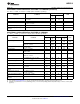
ELECTRICAL CHARACTERISTICS FOR FIXED 3.3V VERSION
V
IN
= 14V, I
O
= 10mA, T
J
= 25°C, C
2
= 100μF (unless otherwise specified)
(1)
LM2931-N-3.3
Parameter Conditions Units
Limit
Typ
(2)
Output Voltage 3.3 3.465 V
MAX
3.135 V
MIN
4V ≤ V
IN
≤ 26V, I
O
= 100 mA 3.630 V
MAX
−40°C ≤ T
J
≤ 125°C 2.970 V
MIN
Line Regulation 4V ≤ V
IN
≤ 26V 4 33 mV
MAX
Load Regulation 5mA ≤ I
O
≤ 100mA 10 50 mV
MAX
Output Impedance 100mA
DC
and 10mA
rms
, 200 mΩ
100Hz - 10kHz
Quiescent Current I
O
≤ 10mA, 4V ≤ V
IN
≤ 26V 0.4 1.0 mA
MAX
−40°C ≤ T
J
≤ 125°C
I
O
= 100mA, V
IN
= 14V, T
J
= 25°C 15 mA
Output Noise Voltage 10Hz -100kHz, C
OUT
= 100μF 330 μV
rms
Long Term Stability 13 mV/1000 hr
Ripple Rejection f
O
= 120Hz 80 dB
(1) See circuit in Typical Applications. To ensure constant junction temperature, low duty cycle pulse testing is used.
(2) All limits are specified for T
J
= 25°C (standard type face) or over the full operating junction temperature range of −40°C to +125°C (bold
type face).
4 Submit Documentation Feedback Copyright © 2000–2013, Texas Instruments Incorporated
Product Folder Links: LM2931-N