
Datasheet


LM317L
www.ti.com
SLCS144D –JULY 2004– REVISED OCTOBER 2011
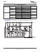
Absolute Maximum Ratings
(1)
over operating temperature range (unless otherwise noted)
MIN MAX UNIT
V
l
– V
O
Input-to-output differential voltage 35 V
D package
(3)
97.1
LP package
(3)
139.5
θ
JA
Package thermal impedance
(2)
°C/W
PK package
(4)
51.5
PW package
(3)
149.4
T
J
Operating virtual-junction temperature 150 °C
T
stg
Storage temperature range –65 150 °C
(1) Stresses beyond those listed under "absolute maximum ratings" may cause permanent damage to the device. These are stress ratings
only, and functional operation of the device at these or any other conditions beyond those indicated under "recommended operating
conditions" is not implied. Exposure to absolute-maximum-rated conditions for extended periods may affect device reliability.
(2) Maximum power dissipation is a function of T
J
(max), θ
JA
, and T
A
. The maximum allowable power dissipation at any allowable ambient
temperature is P
D
= (T
J
(max) – T
A
)/θ
JA
. Operating at the absolute maximum T
J
of 150°C can affect reliability.
(3) The package thermal impedance is calculated in accordance with JESD 51-7.
(4) The package thermal impedance is calculated in accordance with JESD 51-5.
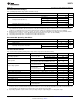
Recommended Operating Conditions
MIN MAX UNIT
V
I
– V
O
Input-to-output voltage differential 35 V
I
O
Output current 2.5 100 mA
LM317LC 0 125
T
J
Operating virtual-junction temperature °C
LM317LI –40 125
Electrical Characteristics
over recommended operating virtual-junction temperature range (unless otherwise noted)
PARAMETER TEST CONDITIONS
(1)
MIN TYP MAX UNIT
T
J
= 25°C 0.01 0.02
Input voltage regulation
(2)
V
I
– V
O
= 5 V to 35 V %V
I
O
= 2.5 mA to 100 mA 0.02 0.05
V
O
= 10 V, f = 120 Hz 65
Ripple regulation dB
V
O
= 10 V,
66 80
10-μF capacitor between ADJUSTMENT and ground
V
O
≤ 5 V 25 mV
V
I
= 5 V to 35 V, T
J
= 25°C,
I
O
= 2.5 mA to 100 mA,
V
O
≥ 5 V 5 mV/V
Output voltage regulation
V
O
≤ 5 V 50 mV
V
I
= 5 V to 35 V,
I
O
= 2.5 mA to 100 mA
V
O
≥ 5 V 10 mV/V
Output voltage change with temperature T
J
= 0°C to 125°C 10 mV/V
Output voltage long-term drift After 1000 hours at T
J
= 125°C and V
I
– V
O
= 35 V 3 10 mV/V
Output noise voltage f = 10 Hz to 10 kHz, T
J
= 25°C 30 μV/V
Minimum output current to maintain regulation V
I
– V
O
= 35 V 1.5 2.5 mA
Peak output current V
I
– V
O
≤ 35 V 100 200 mA
ADJUSTMENT current 50 100 μA
Change in ADJUSTMENT current V
I
– V
O
= 2.5 V to 35 V, I
O
= 2.5 mA to 100 mA 0.2 5 μA
V
I
– V
O
= 5 V to 35 V, I
O
= 2.5 mA to 100 mA,
Reference voltage (output to ADJUSTMENT) 1.2 1.25 1.3 V
P ≤ rated dissipation
(1) Unless otherwise noted, these specifications apply for the following test conditions: V
I
– V
O
= 5 V and I
O
= 40 mA. Pulse-testing
techniques must be used that maintain the junction temperature as close to the ambient temperature as possible. All characteristics are
measured with a 0.1-μF capacitor across the input and a 1-μF capacitor across the output.
(2) Input voltage regulation is expressed here as the percentage change in output voltage per 1-V change at the input.
Copyright © 2004–2011, Texas Instruments Incorporated Submit Documentation Feedback 3
Product Folder Link(s): LM317L