
Datasheet
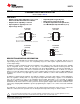
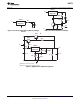


V
O
(see Note A)
R2 = 3 kΩ
1N4002
R3 =
820 Ω
−10 V
C1 = 0.1 µF
35 V
Adjustment
OutputInput
LM317L
NOTE A: Output voltage is calculated from the equation:
where: V
ref
equals the difference between OUTPUT
and ADJUSTMENT voltages (≈1.25 V).
R1 = 120 Ω
V
O
+ V
ref
ǒ
1 )
R2 ) R3
R1
Ǔ
* 10 V
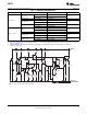
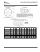
C1 = 0.1 µF
(see Note A)
V
I
470 Ω
R1
R2
C2 = 1 µF
(see Note C)
V
O
(see Note B)
Adjustment
OutputInput
LM317L
NOTES: A. Use of an input bypass capacitor is recommended if
regulator is far from the filter capacitors.
B. Output voltage is calculated from the equation:
where: V
ref
equals the difference between OUTPUT and
ADJUSTMENT voltages (≈1.25 V).
C. Use of an output capacitor improves transient response,
but is optional.
V
O
+ V
ref
ǒ
1 )
R2
R1
Ǔ
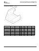
V
I
R1
Adjustment
OutputInput
LM317L
I
limit
+
1.25
R1
R1 =
470 Ω
D1
†
1N4002
C3 = 1 µF
C2 = 10 µF
R2 =
10 kΩ
V
I
+
+
−
−
Adjustment
OutputInput
LM317L
†
D1 discharges C2 if output is shorted to ground.
NOTE A: Use of an output capacitor improves transient response, but is
optional.
V
O
(see Note A)
C1 =
0.1 µF
R3 =
240 Ω
V
I
C1 = 0.1 µF
C2 = 1 µF
Output
Adjust
V
O
R2 = 1.5 kΩ
R1 = 470 Ω
LM317L
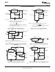
R4 =
2 kΩ
Adjustment
OutputInput
LM317L
Adjustment
OutputInput
R1 =
470 Ω
R2 = 5.1 kΩ
C1 = 25 µF
2N2905
R3 = 50 kΩ
1N4002
V
O
= 15 V
V
I
LM317L
Adjustment
OutputInput
LM317L
SLCS144D –JULY 2004– REVISED OCTOBER 2011
www.ti.com
APPLICATION INFORMATION
Figure 1. Adjustable Voltage Regulator Figure 2. 0-V to 30-V Regulator Circuit
Figure 3. Regulator Circuit With Improved Ripple Figure 4. Precision Current-Limiter Circuit
Rejection
Figure 5. Tracking Preregulator Circuit Figure 6. Slow-Turnon 15-V Regulator Circuit
4 Submit Documentation Feedback Copyright © 2004–2011, Texas Instruments Incorporated
Product Folder Link(s): LM317L