
Datasheet
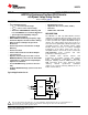
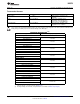
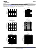

L1:2.2 PH
PGND1
SW1
SGND
V
DD
PGND2
L2:2.2 PH
SW2
SDA
LM3370
V
IN1
V
IN2
C
IN2
4.7 PF
2.7V to 5.5V
C
IN1
4.7 PF
2.7V to 5.5V
FB2
EN2
EN1
FB1
C
OUT1
10 PF
C
OUT2
10 PF
V
OUT2
V
OUT1
SCL
nPOR1
V
IN1
nPOR2
V
IN2
*
* Optional Capacitor
4.7 PF
V
IN1
LM3370
www.ti.com
SNVS406N –NOVEMBER 2005–REVISED MAY 2013
LM3370 Dual Synchronous Step-Down DC-DC Converter
with Dynamic Voltage Scaling Function
Check for Samples: LM3370
1
FEATURES
APPLICATIONS
2
• I
2
C-compatible interface
• Baseband Processors
– V
OUT1
= 1V to 2V in 50 mV Steps • Application Processors (Video, Audio)
– V
OUT2
= 1.8V to 3.3V in 100 mV Steps • I/O Power
– Automatic PFM/PWM Mode Switching and • FPGA Power and CPLD
Forced PWM Mode for Low Noise Operation
DESCRIPTION
– Spread Spectrum Capability Using I
2
C
The LM3370 is a dual step-down DC-DC converter
• 600mA Load Per Channel
optimized for powering ultra-low voltage circuits from
• 2MHz PWM Fixed Switching Frequency (Typ.)
a single Li-Ion battery and input rail ranging from 2.7V
• The Bucks Operate 180° Out-of-Phase Timing
to 5.5V. It provides two outputs with 600mA load per
channel. The output voltage range varies from 1V to
Offset for Noise and Input Surge Current
3.3V and can be dynamically controlled using the I
2
C-
Abatement
compatible interface. This dynamic voltage scaling
• Internal Synchronous Rectification for High
function allows processors to achieve maximum
Efficiency
performance at the lowest power level. The I
2
C-
• Internal Soft Start
compatible interface can also be used to control auto
PFM-PWM/PWM mode selection and other
• Power-on-Reset Function for Both Outputs
performance enhancing features.
• 2.7V ≤ V
IN
≤ 5.5V
The LM3370 offers superior features and
• Operates from a Single Li-Ion Cell or 3 Cell
performance for portable systems with complex
NiMH/NiCd Batteries and 3.3V/5.5V Fixed Rails
power management requirements. Automatic
• 2.2µH Inductor, 4.7µF Input and 10µF Output
intelligent switching between PWM low-noise and
Capacitor Per Channel
PFM low-current mode offers improved system
• 16-lead WSON Package (4 mm x 5 mm x 0.8 efficiency. Internal synchronous rectification
enhances the converter efficiency without the use of
mm)
further external devices.
• 20-Bump DSBGA Package (3.0 mm x 2.0 mm x
0.6 mm)
Typical Application Circuit
1
Please be aware that an important notice concerning availability, standard warranty, and use in critical applications of
Texas Instruments semiconductor products and disclaimers thereto appears at the end of this data sheet.
2All trademarks are the property of their respective owners.
PRODUCTION DATA information is current as of publication date.
Copyright © 2005–2013, Texas Instruments Incorporated
Products conform to specifications per the terms of the Texas
Instruments standard warranty. Production processing does not
necessarily include testing of all parameters.