LM3402, LM3402HV www.ti.com SNVS450E – SEPTEMBER 2006 – REVISED MAY 2013 0.5A Constant Current Buck Regulator for Driving High Power LEDs Check for Samples: LM3402, LM3402HV FEATURES DESCRIPTION • • • • • • • The LM3402/02HV are monolithic switching regulators designed to deliver constant currents to high power LEDs.
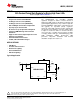
LM3402, LM3402HV SNVS450E – SEPTEMBER 2006 – REVISED MAY 2013 www.ti.com Connection Diagram 1 8 VIN SW 2 BOOT 3 DIM 7 1 6 2 VCC RON 4 GND BOOT 3 5 DIM 4 CS Figure 1. 8-Lead Plastic VSSOP-8 Package See Package Number DGK (S-PDSO-G8) VIN SW GND DAP VCC RON CS 8 7 6 5 Figure 2.
LM3402, LM3402HV www.ti.com SNVS450E – SEPTEMBER 2006 – REVISED MAY 2013 These devices have limited built-in ESD protection. The leads should be shorted together or the device placed in conductive foam during storage or handling to prevent electrostatic damage to the MOS gates. ABSOLUTE MAXIMUM RATINGS(LM3402) (1) If Military/Aerospace specified devices are required, please contact the Texas Instruments Sales Office/ Distributors for availability and specifications. VALUE / UNIT VIN to GND –0.
LM3402, LM3402HV SNVS450E – SEPTEMBER 2006 – REVISED MAY 2013 www.ti.com ABSOLUTE MAXIMUM RATINGS(LM3402HV) (1) VALUE / UNIT VIN to GND −0.3V to 76V BOOT to GND −0.3V to 90V −1.5V SW to GND BOOT to VCC −0.3V to 76V BOOT to SW −0.3V to 14V VCC to GND −0.3V to 14V DIM to GND −0.3V to 7V CS to GND −0.3V to 7V RON to GND −0.3V to 7V Junction Temperature 150°C Storage Temp.
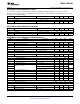
LM3402, LM3402HV www.ti.com SNVS450E – SEPTEMBER 2006 – REVISED MAY 2013 ELECTRICAL CHARACTERISTICS LM3402 VIN = 24V unless otherwise indicated. Typicals and limits appearing in plain type apply for TA = TJ = +25°C. (1) Limits appearing in boldface type apply over full Operating Temperature Range. Datasheet min/max specification limits are ensured by design, test, or statistical analysis.
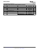
LM3402, LM3402HV SNVS450E – SEPTEMBER 2006 – REVISED MAY 2013 www.ti.com ELECTRICAL CHARACTERISTICS LM3402/LM3402HV (continued) Symbol Parameter Conditions Min Typ Max Units 0.7 1.5 Ω 3 4 V N-MOSFET AND DRIVER RDS-ON Buck Switch On Resistance ISW = 200mA, BOOT-SW = 6.3V VDR-UVLO BOOT Under-voltage Lock-out Threshold BOOT–SW Increasing VDR-HYS BOOT Under-voltage Lock-out Hysteresis BOOT–SW Decreasing 1.
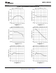
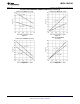
LM3402, LM3402HV www.ti.com SNVS450E – SEPTEMBER 2006 – REVISED MAY 2013 TYPICAL PERFORMANCE CHARACTERISTICS VREF vs Temperature (VIN = 24V) VREF vs VIN, LM3402 (TA = 25°C) Figure 3. Figure 4. VREF vs VIN, LM3402HV (TA = 25°C) Current Limit vs Temperature (VIN = 24V) Figure 5. Figure 6. Current Limit vs VIN, LM3402 (TA = 25°C) Current Limit vs VIN, LM3402HV (TA = 25°C) Figure 7. Figure 8.
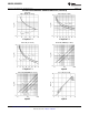
LM3402, LM3402HV SNVS450E – SEPTEMBER 2006 – REVISED MAY 2013 www.ti.com TYPICAL PERFORMANCE CHARACTERISTICS (continued) 8 TON vs VIN, RON = 100 kΩ (TA = 25°C) TON vs VIN, (TA = 25°C) Figure 9. Figure 10. TON vs VIN, (TA = 25°C) TON vs RON, LM3402 (TA = 25°C) Figure 11. Figure 12. TON vs RON, LM3402HV (TA = 25°C) VCC vs VIN (TA = 25°C) Figure 13. Figure 14.
LM3402, LM3402HV www.ti.com SNVS450E – SEPTEMBER 2006 – REVISED MAY 2013 TYPICAL PERFORMANCE CHARACTERISTICS (continued) VO-MAX vs fSW, LM3402 (TA = 25°C) VO-MIN vs fSW, LM3402 (TA = 25°C) Figure 15. Figure 16. VO-MAX vs fSW, LM3402HV (TA = 25°C) VO-MIN vs fSW, LM3402HV (TA = 25°C) Figure 17. Figure 18.
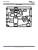
LM3402, LM3402HV SNVS450E – SEPTEMBER 2006 – REVISED MAY 2013 www.ti.com BLOCK DIAGRAM 7V BIAS REGULATOR VIN VIN SENSE VCC UVLO BYPASS SWITCH 0.7V VCC THERMAL SHUTDOWN + 300 ns MIN OFF TIMER Complete ON TIMER RON RON Complete 5V BOOT Start Start GATE DRIVE UVLO 75 PA DIM 1.5V 0.2V + + - SD VIN LEVEL SHIFT LOGIC CS SW 0.3V + - GND 10 Submit Documentation Feedback CURRENT LIMIT OFF TIMER + - 0.
LM3402, LM3402HV www.ti.com SNVS450E – SEPTEMBER 2006 – REVISED MAY 2013 APPLICATION INFORMATION THEORY OF OPERATION The LM3402 and LM3402HV are buck regulators with a wide input voltage range, low voltage reference, and a fast output enable/disable function. These features combine to make them ideal for use as a constant current source for LEDs with forward currents as high as 500 mA.
LM3402, LM3402HV SNVS450E – SEPTEMBER 2006 – REVISED MAY 2013 www.ti.com AVERAGE LED CURRENT ACCURACY The COT architecture regulates the valley of ΔVSNS, the AC portion of VSNS. To determine the average LED current (which is also the average inductor current) the valley inductor current is calculated using the following expression: 0.2 VO x tSNS IL-MIN = L RSNS (4) In this equation tSNS represents the propagation delay of the CS comparator, and is approximately 220 ns.
LM3402, LM3402HV www.ti.com SNVS450E – SEPTEMBER 2006 – REVISED MAY 2013 INTERNAL MOSFET AND DRIVER The LM3402/02HV features an internal power MOSFET as well as a floating driver connected from the SW pin to the BOOT pin. Both rise time and fall time are 20 ns each (typical) and the approximate gate charge is 3 nC. The high-side rail for the driver circuitry uses a bootstrap circuit consisting of an internal high-voltage diode and an external 10 nF capacitor, CB.
LM3402, LM3402HV SNVS450E – SEPTEMBER 2006 – REVISED MAY 2013 www.ti.com CB L1 VIN VIN BOOT SW RON CIN D1 Z1 RON LM3402/02HV RZ CS RSNS DIM VCC GND CF Figure 20. Output Open Circuit Protection LOW POWER SHUTDOWN The LM3402/02HV can be switched to a low power state (IIN-SD = 90 µA) by grounding the RON pin with a signallevel MOSFET as shown in Figure 21. Low power MOSFETs like the 2N7000, 2N3904, or equivalent are recommended devices for putting the LM3402/02HV into low power shutdown.
LM3402, LM3402HV www.ti.com SNVS450E – SEPTEMBER 2006 – REVISED MAY 2013 DESIGN CONSIDERATIONS SWITCHING FREQUENCY Switching frequency is selected based on the tradeoffs between efficiency (better at low frequency), solution size/cost (smaller at high frequency), and the range of output voltage that can be regulated (wider at lower frequency.) Many applications place limits on switching frequency due to EMI sensitivity.
LM3402, LM3402HV SNVS450E – SEPTEMBER 2006 – REVISED MAY 2013 www.ti.com 'iL CO rD 'iC 'iF ESR 'iL RSNS Figure 22. LED and CO Ripple Current To calculate the respective ripple currents the LED array is represented as a dynamic resistance, rD. LED dynamic resistance is not always specified on the manufacturer’s datasheet, but it can be calculated as the inverse slope of the LED’s VF vs. IF curve. Note that dividing VF by IF will give an incorrect value that is 5x to 10x too high.
LM3402, LM3402HV www.ti.com SNVS450E – SEPTEMBER 2006 – REVISED MAY 2013 Ceramic capacitors are the best choice for the input to the LM3402/02HV due to their high ripple current rating, low ESR, low cost, and small size compared to other types. When selecting a ceramic capacitor, special attention must be paid to the operating conditions of the application.
LM3402, LM3402HV SNVS450E – SEPTEMBER 2006 – REVISED MAY 2013 www.ti.com Though most power LEDs are designed to run at several hundred milliamps, some can be seen to glow with a faint light at extremely low current levels, as low as a couple microamps in some instances. In lab testing, the forward voltage was found to be approximately 2V for LEDs that exhibited visible light at these low current levels.
LM3402, LM3402HV www.ti.com SNVS450E – SEPTEMBER 2006 – REVISED MAY 2013 LM3402 SW Module Connector Module Connector VTRANSIENT CS 8V ~ 0.675 GND Figure 24. CS Pin, Transient Path LM3402 SW Module Connector Module Connector VTRANSIENT CS 1 k5 8V ~ 0.675 GND Figure 25. CS Pin, Transient Path with Protection Adding a resistor in series with the CS pin causes the observed output LED current to shift very slightly.
LM3402, LM3402HV SNVS450E – SEPTEMBER 2006 – REVISED MAY 2013 www.ti.com CS PIN PROTECTION WITH OVP When designing output overvoltage protection into the switching converter circuit using a zener diode, transient protection on the CS pin requires additional consideration.
LM3402, LM3402HV www.ti.com SNVS450E – SEPTEMBER 2006 – REVISED MAY 2013 VIN PIN PROTECTION The VIN pin also has an ESD structure from the pin to GND with a breakdown voltage of approximately 80V. Any transient that exceeds this voltage may damage the device. Although transient absorption is usually present at the front end of a switching converter circuit, damage to the VIN pin can still occur.
LM3402, LM3402HV SNVS450E – SEPTEMBER 2006 – REVISED MAY 2013 www.ti.com LM3402 Board Trace Inductance VIN Module Connector 80V TVS VIN CIN TVS or smaller zener diode GND Module Connector Figure 29. VIN Pin with Additional Input Protection GENERAL COMMENTS REGARDING OTHER PINS Any pin that goes “off-board” through a connector should have series resistance of at least 1kΩ to 10kΩ in series with it to protect it from ESD or other transients.
LM3402, LM3402HV www.ti.com SNVS450E – SEPTEMBER 2006 – REVISED MAY 2013 CB L1 VIN = 24V VIN BOOT SW RON CIN D1 RON CO LED1 IF = 350 mA LM3402/02HV CS DIM RSNS VCC GND CF Figure 30. Schematic for Design Example 1 RON and tON To select RON the expression relating tON to input voltage from the Controlled On-time Overview section can be re-written as: tON x VIN RON = 1.34 x 10⁻¹⁰ (18) Minimum on-time occurs at the maximum VIN, which is 24V x 110% = 26.4V.
LM3402, LM3402HV SNVS450E – SEPTEMBER 2006 – REVISED MAY 2013 www.ti.com Inductor datasheets should contain three specifications which are used to select the inductor. The first of these is the average current rating, which for a buck regulator is equal to the average load current, or IF. The average current rating is given by a specified temperature rise in the inductor, normally 40°C.
LM3402, LM3402HV www.ti.com SNVS450E – SEPTEMBER 2006 – REVISED MAY 2013 CO = 1/(2 x π x 0.157 x 4.68 x 105) = 2.18 µF (34) This calculation assumes that impedance due to the equivalent series resistance (ESR) and equivalent series inductance (ESL) of CO is negligible. The closest 10% tolerance capacitor value is 2.2 µF. The capacitor used should be rated to 10V or more and have an X7R dielectric. Several manufacturers produce ceramic capacitors with these specifications in the 0805 case size.
LM3402, LM3402HV SNVS450E – SEPTEMBER 2006 – REVISED MAY 2013 www.ti.com Gate charging and VCC loss, PG, in the gate drive and linear regulator: PG = (IIN-OP + fSW x QG) x VIN PG = (600 x 10-6 + 468000 x 3 x 10-9) x 24 = 48 mW (41) Switching loss, PS, in the internal MOSFET: PS = 0.5 x VIN x IF x (tR + tF) x fSW PS = 0.5 x 24 x 0.35 x (40 x 10-9) x 468000 = 78 mW (42) AC rms current loss, PCIN, in the input capacitor: PCIN = IIN(rms)2 x ESR = (0.126)2 x 0.006 = 0.
LM3402, LM3402HV www.ti.com SNVS450E – SEPTEMBER 2006 – REVISED MAY 2013 OUTPUT INDUCTOR In this example the ripple current through the LED array and the inductor are equal. Inductance is selected to give the smallest ripple current possible while still providing enough ΔvSNS signal for the CS comparator to operate correctly.
LM3402, LM3402HV SNVS450E – SEPTEMBER 2006 – REVISED MAY 2013 www.ti.com In expectation that more capacitance will be needed to prevent power supply interaction a 2.2 µF ceramic capacitor rated to 100V with X7R dielectric in an 1812 case size will be used. From the Design Considerations section, input rms current is: IIN-RMS = 0.35 x Sqrt(0.82 x 0.18) = 134 mA (66) Ripple current ratings for 1812 size ceramic capacitors are typically higher than 2A, more than enough for this design.
LM3402, LM3402HV www.ti.com SNVS450E – SEPTEMBER 2006 – REVISED MAY 2013 Layout Considerations The performance of any switching converter depends as much upon the layout of the PCB as the component selection. The following guidelines will help the user design a circuit with maximum rejection of outside EMI and minimum generation of unwanted EMI.
LM3402, LM3402HV SNVS450E – SEPTEMBER 2006 – REVISED MAY 2013 www.ti.com Table 1. BOM for Design Example 1 ID Part Number Type Size Parameters Qty Vendor U1 LM3402 LED Driver VSSOP-8 40V, 0.5A 1 NSC L1 SLF7045T-330MR82 Inductor 7.0x7.0 x4.5mm 33µH, 0.82A, 96mΩ 1 TDK D1 CMHSH5-4 Schottky Diode SOD-123 40V, 0.
LM3402, LM3402HV www.ti.com SNVS450E – SEPTEMBER 2006 – REVISED MAY 2013 REVISION HISTORY Changes from Revision D (May 2013) to Revision E • Page Changed layout of National Data Sheet to TI format ..........................................................................................................
PACKAGE OPTION ADDENDUM www.ti.
PACKAGE OPTION ADDENDUM www.ti.com 18-Oct-2013 (3) MSL, Peak Temp. - The Moisture Sensitivity Level rating according to the JEDEC industry standard classifications, and peak solder temperature. (4) There may be additional marking, which relates to the logo, the lot trace code information, or the environmental category on the device. (5) Multiple Device Markings will be inside parentheses. Only one Device Marking contained in parentheses and separated by a "~" will appear on a device.
PACKAGE MATERIALS INFORMATION www.ti.com 28-Sep-2013 TAPE AND REEL INFORMATION *All dimensions are nominal Device Package Package Pins Type Drawing SPQ Reel Reel A0 Diameter Width (mm) (mm) W1 (mm) B0 (mm) K0 (mm) P1 (mm) W Pin1 (mm) Quadrant LM3402HVMMX/NOPB VSSOP DGK 8 3500 330.0 12.4 5.3 3.4 1.4 8.0 12.0 Q1 LM3402HVMRX/NOPB SO Power PAD DDA 8 2500 330.0 12.4 6.5 5.4 2.0 8.0 12.0 Q1 LM3402MRX/NOPB SO Power PAD DDA 8 2500 330.0 12.4 6.5 5.4 2.0 8.0 12.
PACKAGE MATERIALS INFORMATION www.ti.com 28-Sep-2013 *All dimensions are nominal Device Package Type Package Drawing Pins SPQ Length (mm) Width (mm) Height (mm) LM3402HVMMX/NOPB VSSOP DGK 8 3500 367.0 367.0 35.0 LM3402HVMRX/NOPB SO PowerPAD DDA 8 2500 367.0 367.0 35.0 LM3402MRX/NOPB SO PowerPAD DDA 8 2500 367.0 367.0 35.
MECHANICAL DATA DDA0008B MRA08B (Rev B) www.ti.
IMPORTANT NOTICE Texas Instruments Incorporated and its subsidiaries (TI) reserve the right to make corrections, enhancements, improvements and other changes to its semiconductor products and services per JESD46, latest issue, and to discontinue any product or service per JESD48, latest issue. Buyers should obtain the latest relevant information before placing orders and should verify that such information is current and complete.