LM3404, LM3404HV www.ti.com SNVS465F – OCTOBER 2006 – REVISED MAY 2013 1.0A Constant Current Buck Regulator for Driving High Power LEDs Check for Samples: LM3404, LM3404HV FEATURES DESCRIPTION • • • • • • • The LM3404/04HV are monolithic switching regulators designed to deliver constant currents to high power LEDs. Ideal for automotive, industrial, and general lighting applications, they contain a high-side N-channel MOSFET switch with a current limit of 1.5A (typical) for step-down (Buck) regulators.
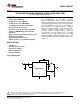
LM3404, LM3404HV SNVS465F – OCTOBER 2006 – REVISED MAY 2013 www.ti.com Connection Diagrams 1 8 VIN SW 2 7 1 6 2 VCC BOOT 3 DIM RON 4 GND BOOT 3 5 DIM 4 CS Figure 1. 8-Lead Plastic SOIC-8 Package VIN SW GND DAP VCC RON CS 8 7 6 5 Figure 2. 8-Lead Plastic So PowerPAD-8 Package PIN DESCRIPTIONS 2 Pin(s) Name 1 SW 2 BOOT 3 DIM 4 GND 5 CS 6 7 8 VIN DAP GND Description Application Information Switch pin Connect this pin to the output inductor and Schottky diode.
LM3404, LM3404HV www.ti.com SNVS465F – OCTOBER 2006 – REVISED MAY 2013 These devices have limited built-in ESD protection. The leads should be shorted together or the device placed in conductive foam during storage or handling to prevent electrostatic damage to the MOS gates. ABSOLUTE MAXIMUM RATINGS(LM3404) (1) If Military/Aerospace specified devices are required, please contact the Texas Instruments Semiconductor Sales Office/ Distributors for availability and specifications.
LM3404, LM3404HV SNVS465F – OCTOBER 2006 – REVISED MAY 2013 www.ti.com ABSOLUTE MAXIMUM RATINGS (LM3404HV) (1) VALUE / UNIT VIN to GND –0.3 V to 76 V BOOT to GND –0.3 V to 90 V SW to GND –1.5 V to 76 V BOOT to VCC –0.3 V to 76 V BOOT to SW –0.3 V to 14 V VCC to GND –0.3 V to 14 V DIM to GND –0.3 V to 7 V CS to GND –0.3 V to 7 V RON to GND –0.
LM3404, LM3404HV www.ti.com SNVS465F – OCTOBER 2006 – REVISED MAY 2013 ELECTRICAL CHARACTERISTICS LM3404 VIN = 24V unless otherwise indicated. Typicals and limits appearing in plain type apply for TA = TJ = 25°C. (1) Limits appearing in boldface type apply over full Operating Temperature Range. Datasheet min/max specification limits are specified by design, test, or statistical analysis. Symbol Parameter Conditions Min Typ Max Units SYSTEM PARAMETERS tON-1 On-time 1 VIN = 10V, RON = 200 kΩ 2.
LM3404, LM3404HV SNVS465F – OCTOBER 2006 – REVISED MAY 2013 www.ti.com LM3404/LM3404HV(1) (continued) Symbol Parameter Conditions Min Typ Max Units 0.37 0.75 Ω 3 4 V MOSFET AND DRIVER RDS-ON Buck Switch On Resistance ISW = 200mA, BST-SW = 6.3V VDR-UVLO BST Under-voltage Lock-out Threshold BST–SW Increasing VDR-HYS BST Under-voltage Lock-out Hysteresis BST–SW Decreasing 1.
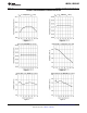
LM3404, LM3404HV www.ti.com SNVS465F – OCTOBER 2006 – REVISED MAY 2013 TYPICAL PERFORMANCE CHARACTERISTICS spacer VREF vs Temperature (VIN = 24V) VREF vs VIN, LM3404 (TA = 25°C) Figure 3. Figure 4. VREF vs VIN, LM3404HV (TA = 25°C) Current Limit vs Temperature (VIN = 24V) Figure 5. Figure 6. Current Limi vs VIN, LM3404 (TA = 25°C) Current Limit vs VIN, LM3404HV (TA = 25°C) Figure 7. Figure 8.
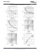
LM3404, LM3404HV SNVS465F – OCTOBER 2006 – REVISED MAY 2013 www.ti.com TYPICAL PERFORMANCE CHARACTERISTICS (continued) spacer 8 TON vs VIN, RON = 100 kΩ (TA = 25°C) TON vs VIN, (TA = 25°C) Figure 9. Figure 10. TON vs VIN, (TA = 25°C) TON vs RON, LM3404 (TA = 25°C) Figure 11. Figure 12. TON vs RON, LM3404HV (TA = 25°C) VCC vs VIN (TA = 25°C) Figure 13. Figure 14.
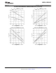
LM3404, LM3404HV www.ti.com SNVS465F – OCTOBER 2006 – REVISED MAY 2013 TYPICAL PERFORMANCE CHARACTERISTICS (continued) spacer VO-MAX vs fSW, LM3404 (TA = 25°C) VO-MIN vs fSW, LM3404 (TA = 25°C) Figure 15. Figure 16. VO-MAX vs fSW, LM3404HV (TA = 25°C) VO-MIN vs fSW, LM3404HV (TA = 25°C) Figure 17. Figure 18.
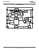
LM3404, LM3404HV SNVS465F – OCTOBER 2006 – REVISED MAY 2013 www.ti.com BLOCK DIAGRAM 7V BIAS REGULATOR VIN VIN SENSE VCC UVLO BYPASS SWITCH 0.7V VCC THERMAL SHUTDOWN + 300 ns MIN OFF TIMER Complete ON TIMER RON RON Complete 5V BOOT Start Start GATE DRIVE SD UVLO 75 PA DIM 1.5V 0.2V + + - VIN LEVEL SHIFT LOGIC CS SW 0.3V + - GND 10 Submit Documentation Feedback CURRENT LIMIT OFF TIMER + - 1.
LM3404, LM3404HV www.ti.com SNVS465F – OCTOBER 2006 – REVISED MAY 2013 APPLICATION INFORMATION THEORY OF OPERATION The LM3404 and LM3404HV are buck regulators with a wide input voltage range, low voltage reference, and a fast output enable/disable function. These features combine to make them ideal for use as a constant current source for LEDs with forward currents as high as 1.2A.
LM3404, LM3404HV SNVS465F – OCTOBER 2006 – REVISED MAY 2013 www.ti.com AVERAGE LED CURRENT ACCURACY The COT architecture regulates the valley of ΔVSNS, the AC portion of VSNS. To determine the average LED current (which is also the average inductor current) the valley inductor current is calculated using the following expression: 0.2 VO x tSNS IL-MIN = L RSNS (3) In this equation tSNS represents the propagation delay of the CS comparator, and is approximately 220 ns.
LM3404, LM3404HV www.ti.com SNVS465F – OCTOBER 2006 – REVISED MAY 2013 INTERNAL MOSFET AND DRIVER The LM3404/04HV features an internal power MOSFET as well as a floating driver connected from the SW pin to the BOOT pin. Both rise time and fall time are 20 ns each (typical) and the approximate gate charge is 6 nC. The high-side rail for the driver circuitry uses a bootstrap circuit consisting of an internal high-voltage diode and an external 10 nF capacitor, CB.
LM3404, LM3404HV SNVS465F – OCTOBER 2006 – REVISED MAY 2013 www.ti.com CB VIN VIN BOOT L1 SW RON CIN D1 Z1 RON LM3404/04HV RZ CS RSNS DIM GND VCC CF Figure 20. Output Open Circuit Protection LOW POWER SHUTDOWN The LM3404/04HV can be placed into a low power state (IIN-SD = 90 µA) by grounding the RON pin with a signallevel MOSFET as shown in Figure 21. Low power MOSFETs like the 2N7000, 2N3904, or equivalent are recommended devices for putting the LM3404/04HV into low power shutdown.
LM3404, LM3404HV www.ti.com SNVS465F – OCTOBER 2006 – REVISED MAY 2013 DESIGN CONSIDERATIONS SWITCHING FREQUENCY Switching frequency is selected based on the trade-offs between efficiency (better at low frequency), solution size/cost (smaller at high frequency), and the range of output voltage that can be regulated (wider at lower frequency.) Many applications place limits on switching frequency due to EMI sensitivity.
LM3404, LM3404HV SNVS465F – OCTOBER 2006 – REVISED MAY 2013 www.ti.com 'iL CO rD 'iC 'iF ESR 'iL RSNS Figure 22. LED and CO Ripple Current To calculate the respective ripple currents the LED array is represented as a dynamic resistance, rD. LED dynamic resistance is not always specified on the manufacturer’s datasheet, but it can be calculated as the inverse slope of the LED’s VF vs. IF curve. Note that dividing VF by IF will give an incorrect value that is 5x to 10x too high.
LM3404, LM3404HV www.ti.com SNVS465F – OCTOBER 2006 – REVISED MAY 2013 A good starting point for selection of CIN is to use an input voltage ripple of 5% to 10% of VIN. A minimum input capacitance of 2x the CIN(MIN) value is recommended for all LM3404/04HV circuits.
LM3404, LM3404HV SNVS465F – OCTOBER 2006 – REVISED MAY 2013 www.ti.com 25 SW CURRENT (PA) 20 15 10 5 0 0 1 2 3 4 5 6 SW VOLTAGE (V) Figure 23. LED Current From SW Pin Though most power LEDs are designed to run at several hundred milliamps, some can be seen to glow with a faint light at extremely low current levels, as low as a couple microamps in some instances.
LM3404, LM3404HV www.ti.com SNVS465F – OCTOBER 2006 – REVISED MAY 2013 CS PIN PROTECTION When hot swapping in a load (e.g. test points, load boards, LED stack), any residual charge on the load will be immediately transferred through the output capacitor to the CS pin, which is then damaged as shown in Figure 24 below. The EOS event due to the residual charge from the load is represented as VTRANSIENT.
LM3404, LM3404HV SNVS465F – OCTOBER 2006 – REVISED MAY 2013 www.ti.com LM3404 SW Module Connector Module Connector VTRANSIENT CS 1 k5 8V ~ 0.675 GND Figure 25. CS Pin, Transient Path with Protection Adding a resistor in series with the CS pin causes the observed output LED current to shift very slightly.
LM3404, LM3404HV www.ti.com SNVS465F – OCTOBER 2006 – REVISED MAY 2013 LM3404 SW Module Connector Module Connector VTRANSIENT CS 1 k5 8V ~ 0.675 GND Figure 26. CS Pin with OVP, Transient Path LM3404 SW Module Connector Module Connector VTRANSIENT CS 1 k5 5005 8V ~ 0.675 GND Figure 27.
LM3404, LM3404HV SNVS465F – OCTOBER 2006 – REVISED MAY 2013 www.ti.com VIN PIN PROTECTION The VIN pin also has an ESD structure from the pin to GND with a breakdown voltage of approximately 80V. Any transient that exceeds this voltage may damage the device. Although transient absorption is usually present at the front end of a switching converter circuit, damage to the VIN pin can still occur.
LM3404, LM3404HV www.ti.com SNVS465F – OCTOBER 2006 – REVISED MAY 2013 LM3404 Board Trace Inductance VIN Module Connector 80V CIN TVS VIN TVS or smaller zener diode GND Module Connector Figure 29. VIN Pin with Additional Input Protection GENERAL COMMENTS REGARDING OTHER PINS Any pin that goes “off-board” through a connector should have series resistance of at least 1kΩ to 10kΩ in series with it to protect it from ESD or other transients.
LM3404, LM3404HV SNVS465F – OCTOBER 2006 – REVISED MAY 2013 www.ti.com CB VIN = 24V VIN BOOT SW RON CIN IF = 700 mA L1 D1 RON CO LED1 LM3404 CS RSNS DIM GND VCC CF Figure 30. Schematic for Design Example 1 RON and tON A moderate switching frequency is needed in this application to balance the requirements of magnetics size and efficiency. RON is selected from the equation for switching frequency as follows: VO RON = 1.34 x 10⁻¹⁰ x fSW (17) (18) RON = 7.1 / (1.34 x 10-10 x 4 x 105) = 132.
LM3404, LM3404HV www.ti.com SNVS465F – OCTOBER 2006 – REVISED MAY 2013 The peak LED/inductor current is then estimated: IL(PEAK) = IL + 0.5 x ΔiL(MAX) IL(PEAK) = 0.7 + 0.5 x 0.330 = 866 mA (27) (28) In the case of a short circuit across the LED array, the LM3404 will continue to deliver rated current through the short but will reduce the output voltage to equal the CS pin voltage of 200 mV. The inductor ripple current and peak current in this condition would be equal to: ΔiL(LED-SHORT) = [(24 – 0.
LM3404, LM3404HV SNVS465F – OCTOBER 2006 – REVISED MAY 2013 www.ti.com To provide additional safety margin the a higher value of 3.3 µF ceramic capacitor rated to 50V with X7R dielectric in an 1210 case size will be used. From the Design Considerations section, input rms current is: IIN-RMS = 0.7 x Sqrt(0.28 x 0.72) = 314 mA (39) Ripple current ratings for 1210 size ceramic capacitors are typically higher than 2A, more than enough for this design.
LM3404, LM3404HV www.ti.com SNVS465F – OCTOBER 2006 – REVISED MAY 2013 Design Example 2: LM3404HV The second example circuit will guide the user through component selection for an outdoor general lighting application. A regulated DC voltage input of 48V ±10% will power ten series-connected LEDs at 500 mA ±10% with a ripple current of 50 mAP-P or less. The typical forward voltage of the LED module in thermal steady state is 35V, hence the average output voltage will be 35.2V.
LM3404, LM3404HV SNVS465F – OCTOBER 2006 – REVISED MAY 2013 www.ti.com The closest standard inductor value above 281 is 330 µH. The average current rating should be greater than 0.5A to prevent overheating in the inductor. In this example the LM3404HV driver and the LED array share the same metal-core PCB, meaning that heat from the inductor could threaten the lifetime of the LEDs. For this reason the average current rating of the inductor used should have a de-rating of about 50%, or 1A.
LM3404, LM3404HV www.ti.com SNVS465F – OCTOBER 2006 – REVISED MAY 2013 RSNS A preliminary value for RSNS was determined in selecting ΔiL. This value should be re-evaluated based on the calculations for ΔiF: 0.2 x L RSNS = IF x L + VO x tSNS - VIN - VO x tON 2 (67) (68) tSNS = 220 ns, RSNS = 0.43Ω Sub-1Ω resistors are available in both 1% and 5% tolerance. A 1%, 0.43Ω device is the closest value, and a 0.25W, 0805 size device will handle the power dissipation of 110 mW.
LM3404, LM3404HV SNVS465F – OCTOBER 2006 – REVISED MAY 2013 www.ti.com Conduction loss, PC, in the internal MOSFET: PC = (IF2 x RDSON) x D = (0.52 x 0.8) x 0.73 = 146 mW (75) Gate charging and VCC loss, PG, in the gate drive and linear regulator: PG = (IIN-OP + fSW x QG) x VIN PG = (600 x 10-6 + 2.23 x 105 x 6 x 10-9) x 48 = 94 mW (76) Switching loss, PS, in the internal MOSFET: PS = 0.5 x VIN x IF x (tR + tF) x fSW PS = 0.5 x 48 x 0.5 x 40 x 10-9 x 2.
LM3404, LM3404HV www.ti.com SNVS465F – OCTOBER 2006 – REVISED MAY 2013 any other circuit path. The continuous current paths on the ground net can be routed on the system ground plane with less risk of injecting noise into other circuits. The path between the input source and the input capacitor and the path between the recirculating diode and the LEDs/current sense resistor are examples of continuous current paths.
LM3404, LM3404HV SNVS465F – OCTOBER 2006 – REVISED MAY 2013 www.ti.com REVISION HISTORY Changes from Revision E (May 2013) to Revision F • 32 Page Changed layout of National Data Sheet to TI format ..........................................................................................................
PACKAGE OPTION ADDENDUM www.ti.
PACKAGE OPTION ADDENDUM www.ti.com (4) 5-Feb-2014 There may be additional marking, which relates to the logo, the lot trace code information, or the environmental category on the device. (5) Multiple Device Markings will be inside parentheses. Only one Device Marking contained in parentheses and separated by a "~" will appear on a device. If a line is indented then it is a continuation of the previous line and the two combined represent the entire Device Marking for that device.
PACKAGE MATERIALS INFORMATION www.ti.com 29-May-2013 TAPE AND REEL INFORMATION *All dimensions are nominal Device Package Package Pins Type Drawing SPQ Reel Reel A0 Diameter Width (mm) (mm) W1 (mm) B0 (mm) K0 (mm) P1 (mm) W Pin1 (mm) Quadrant LM3404HVMAX/NOPB SOIC D 8 2500 330.0 12.4 6.5 5.4 2.0 8.0 12.0 Q1 LM3404HVMRX/NOPB SO Power PAD DDA 8 2500 330.0 12.4 6.5 5.4 2.0 8.0 12.0 Q1 LM3404MAX/NOPB SOIC D 8 2500 330.0 12.4 6.5 5.4 2.0 8.0 12.
PACKAGE MATERIALS INFORMATION www.ti.com 29-May-2013 *All dimensions are nominal Device Package Type Package Drawing Pins SPQ Length (mm) Width (mm) Height (mm) LM3404HVMAX/NOPB SOIC D 8 2500 367.0 367.0 35.0 LM3404HVMRX/NOPB SO PowerPAD DDA 8 2500 367.0 367.0 35.0 LM3404MAX/NOPB SOIC D 8 2500 367.0 367.0 35.0 LM3404MRX/NOPB SO PowerPAD DDA 8 2500 367.0 367.0 35.
MECHANICAL DATA DDA0008B MRA08B (Rev B) www.ti.
IMPORTANT NOTICE Texas Instruments Incorporated and its subsidiaries (TI) reserve the right to make corrections, enhancements, improvements and other changes to its semiconductor products and services per JESD46, latest issue, and to discontinue any product or service per JESD48, latest issue. Buyers should obtain the latest relevant information before placing orders and should verify that such information is current and complete.