LM3409, LM3409HV, LM3409-Q1 www.ti.com SNVS602J – MARCH 2009 – REVISED MAY 2013 PFET Buck Controller for High Power LED Drivers Check for Samples: LM3409, LM3409HV, LM3409-Q1 FEATURES DESCRIPTION • The LM3409/09N/09HV/09Q/09QHV are P-channel MosFET (PFET) controllers for step-down (buck) current regulators. They offer wide input voltage range, high-side differential current sense with low adjustable threshold voltage and fast output enable/disable function and a thermally enhanced VSSOP-10 package.
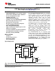
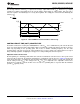
LM3409, LM3409HV, LM3409-Q1 SNVS602J – MARCH 2009 – REVISED MAY 2013 www.ti.com Connection Diagram LM3409/09Q/09HV/09QHV 1 2 3 4 5 UVLO VIN IADJ VCC EN DAP COFF GND CSP CSN PGATE LM3409N 10 1 9 2 8 3 7 4 6 5 6 7 Figure 1. 10-Lead VSSOP Package UVLO VIN NC NC IADJ VCC EN CSP COFF CSN GND NC PGATE NC 14 13 12 11 10 9 8 Figure 2.
LM3409, LM3409HV, LM3409-Q1 www.ti.com SNVS602J – MARCH 2009 – REVISED MAY 2013 Absolute Maximum RatingsLM3409/09N/09Q/09HV/09QHV (1) (2) VIN, EN, UVLO to GND -0.3V to 45V (76V LM3409HV/09QHV) VIN to VCC, PGATE -0.3V to 7V VIN to PGATE -2.8V for 100ns 9.5V for 100ns VIN to CSP, CSN -0.3V to 0.3V COFF to GND -0.
LM3409, LM3409HV, LM3409-Q1 SNVS602J – MARCH 2009 – REVISED MAY 2013 www.ti.com Electrical Characteristics LM3409/09N/09Q/09HV/09QHV (continued) VIN = 24V unless otherwise indicated. Typicals and limits appearing in plain type apply for TA = TJ = +25°C (1). Limits appearing in boldface type apply over full Operating Temperature Range. Datasheet min/max specification limits are specified by design, test, or statistical analysis.
LM3409, LM3409HV, LM3409-Q1 www.ti.com SNVS602J – MARCH 2009 – REVISED MAY 2013 Typical Performance Characteristics TA = +25°C, VIN = 24V, and characteristics are identical for LM3409 and LM3409HV unless otherwise specified. VCC vs. Junction Temperature 6.125 248 6.100 VCC (V) VCST (mV) VCST vs. Junction Temperature 250 246 244 242 -50 6.075 6.050 -14 22 58 94 6.025 -50 130 94 TEMPERATURE (°C) Figure 4. 1.255 -5.10 1.250 -5.15 1.245 -5.20 1.240 -5.25 1.235 -5.
LM3409, LM3409HV, LM3409-Q1 SNVS602J – MARCH 2009 – REVISED MAY 2013 www.ti.com Typical Performance Characteristics (continued) TA = +25°C, VIN = 24V, and characteristics are identical for LM3409 and LM3409HV unless otherwise specified. LM3409 Efficiency vs. Input Voltage VO = 10V (3 LEDs); ILED = 2A (1) LM3409HV Efficiency vs.
LM3409, LM3409HV, LM3409-Q1 www.ti.com SNVS602J – MARCH 2009 – REVISED MAY 2013 Typical Performance Characteristics (continued) TA = +25°C, VIN = 24V, and characteristics are identical for LM3409 and LM3409HV unless otherwise specified. 2.3 Internal EN Pin PWM Dimming VO = 17V (5 LEDs); VIN = 24V External Parallel FET PWM Dimming VO = 17V (5 LEDs); VIN = 24V 2.3 1.8 1.8 20kHz 100 kHz 1.4 ILED (A) 0.9 0.9 1kHz 50 kHz 0.5 20 40 60 80 0.
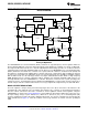
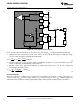
LM3409, LM3409HV, LM3409-Q1 SNVS602J – MARCH 2009 – REVISED MAY 2013 www.ti.com BLOCK DIAGRAM VCC REGULATOR VIN VCC VIN OFF TIMER COFF Complete COFF VCC UVLO THERMAL SHUTDOWN PGATE Start VCC EN R CSN + LOGIC CSP R 22 #A 1.24V + UVLO 5 #A + - IADJ 1.24V GND 5R Theory of Operation The LM3409/09HV are P-channel MosFET (PFET) controllers for step-down (buck) current regulators which are ideal for driving LED loads.
LM3409, LM3409HV, LM3409-Q1 www.ti.com SNVS602J – MARCH 2009 – REVISED MAY 2013 The average inductor current (IL) is equal to the average output LED current (ILED), therefore if IL is tightly controlled, ILED will be well regulated. As the system changes input voltage or output voltage, duty cycle (D) is varied to regulate IL and ultimately ILED.
LM3409, LM3409HV, LM3409-Q1 SNVS602J – MARCH 2009 – REVISED MAY 2013 www.ti.com V IN LM3409/09HV R CSP + V CST + + R SNS - t ON ENDS - VSNS CSN R IT PGATE 5V Q1 L1 IL LED+ 5 #A IADJ + - + 1.24 V VADJ - R EXT Optional D1 LED- GND 5R Figure 22. Peak Current Control Circuit There are three different methods to set the current sense threshold (VCST) using the multi-function IADJ pin: 1.
LM3409, LM3409HV, LM3409-Q1 www.ti.com SNVS602J – MARCH 2009 – REVISED MAY 2013 VO LM3409/09HV ROFF + tOFF Control Logic - to PGATE Drive COFF 1.24V COFF + vCOFF - Figure 23. Off-Time Control Circuit At the start of tOFF, the voltage across COFF (vCOFF(t)) is zero and the capacitor begins charging according to the time constant provided by ROFF and COFF. When vCOFF(t) reaches the off-time threshold (VOFT = 1.24V), then the off-time is terminated and vCOFF(t) is reset to zero.
LM3409, LM3409HV, LM3409-Q1 SNVS602J – MARCH 2009 – REVISED MAY 2013 www.ti.com Using the actual tOFF equation, the inductor current ripple (ΔiL-PP) of a buck current regulator operating in CCM is: § 1. 24V · ¸ - VO x R OFF x (COFF + 20 pF) x ln ¨¨1 VO ¸¹ © ' iL - PP = L1 (7) Using the tOFF approximation, the equation is reduced to: 'iL - PP | 1.
LM3409, LM3409HV, LM3409-Q1 www.ti.com SNVS602J – MARCH 2009 – REVISED MAY 2013 iL(t) IL-MAX-H IL-MAX IL-MAX-L 0 tOFF 0 t tOFF Figure 26. Inductor Current iL(t) Showing IL-MAX Offset INDUCTOR CURRENT RIPPLE Because the LM3409/09HV swaps the polarity of the differential current sense comparator every cycle, a minimum inductor current ripple (ΔiL-PP) is necessary to maintain accurate ILED regulation.
LM3409, LM3409HV, LM3409-Q1 SNVS602J – MARCH 2009 – REVISED MAY 2013 www.ti.com iLED (t) ILED-MAX ILED IDIM-LED DDIM x TDIM t 0 tOFF TDIM Figure 27. LED Current iLED(t) During EN Pin PWM Dimming PWM DIMMING USING THE EN PIN The enable pin (EN) is a TTL compatible input for PWM dimming of the LED. A logic low (below 0.5V) at EN will disable the internal driver and shut off the current flow to the LED array.
LM3409, LM3409HV, LM3409-Q1 www.ti.com SNVS602J – MARCH 2009 – REVISED MAY 2013 LM3409/09HV VIN 22 #A RUV2 + - ON/OFF UVLO 1.24V RUV1 Figure 28. UVLO Circuit The turn-on threshold (VTURN-ON) is defined as follows: VTURN-ON = 1. 24V x (RUV1 + RUV2) RUV1 (16) The hysteresis (VHYS) is defined as follows: VHYS = RUV2 x 22 PA (17) LOW POWER SHUTDOWN The LM3409/09HV can be placed into a low power shutdown (typically 110µA) by grounding the EN terminal (any voltage below 0.
LM3409, LM3409HV, LM3409-Q1 SNVS602J – MARCH 2009 – REVISED MAY 2013 www.ti.com BUCK CONVERTERS W/O OUTPUT CAPACITORS Because current is being regulated, not voltage, a buck current regulator is free of load current transients, therefore output capacitance is not needed to supply the load and maintain output voltage. This is very helpful when high frequency PWM dimming the LED load. When no output capacitor is used, the same design equations that govern ΔiL-PP also apply to ΔiLED-PP.
LM3409, LM3409HV, LM3409-Q1 www.ti.com SNVS602J – MARCH 2009 – REVISED MAY 2013 OUTPUT OVER-VOLTAGE PROTECTION Because the LM3409/09HV controls a buck current regulator, there is no inherent need to provide output overvoltage protection. If the LED load is opened, the output voltage will only rise as high as the input voltage plus any ringing due to the parasitic inductance and capacitance present at the output node.
LM3409, LM3409HV, LM3409-Q1 SNVS602J – MARCH 2009 – REVISED MAY 2013 www.ti.com A good rule of thumb is to limit Qg < 30nC (if the switching frequency remains below 300kHz for the entire operating range then a larger Qg can be considered). If a PFET with small RDS-ON and a high voltage rating is required, there may be no choice but to use a PFET with Qg > 30nC. When using a PFET with Qg > 30nC, the bypass capacitor (CF) should not be connected to the VIN pin.
LM3409, LM3409HV, LM3409-Q1 www.ti.com SNVS602J – MARCH 2009 – REVISED MAY 2013 LM3409/09HV VDD > 1.6V REXT EN CEXT ILED VDD Dim FET PWM Gate Driver Figure 31. External Parallel FET Dimming Circuit As shown in Figure 31, a small capacitor (CEXT) is connected from the gate drive signal of the parallel Dim FET to the EN pin and a pull-up resistor (REXT) is placed from the EN pin to the external VDD supply for the Dim FET gate driver.
LM3409, LM3409HV, LM3409-Q1 SNVS602J – MARCH 2009 – REVISED MAY 2013 www.ti.
LM3409, LM3409HV, LM3409-Q1 www.ti.com R OFF = SNVS602J – MARCH 2009 – REVISED MAY 2013 § VO · ¸ - ¨¨1¸ © K x VIN ¹ · § (COFF + 20 pF) x fSW x ln ¨¨1 - 1.24V ¸¸ V O ¹ © (28) 2. INDUCTOR RIPPLE CURRENT Set the inductor ripple current (ΔiL-PP) by solving for the appropriate inductor (L1): V xt L1 = O OFF 'iL- PP (29) 3.
LM3409, LM3409HV, LM3409-Q1 SNVS602J – MARCH 2009 – REVISED MAY 2013 www.ti.com 6.
LM3409, LM3409HV, LM3409-Q1 www.ti.com SNVS602J – MARCH 2009 – REVISED MAY 2013 'i · § ¨ILED + L-PP¸ x RSNS 2 ¹ REXT = © 1 PA (44) 10. PWM DIMMING METHOD There are two methods to PWM dim using the LM3409/09HV: Method #1: Apply an external PWM signal to the EN terminal. Method #2: Perform external parallel FET shunt dimming as detailed in the EXTERNAL PARALLEL FET PWM DIMMING section.
LM3409, LM3409HV, LM3409-Q1 SNVS602J – MARCH 2009 – REVISED MAY 2013 ROFF = www.ti.com § VO · ¸ - ¨¨1¸ © K x VIN ¹ § 1.24V· ¸ (COFF + 20 pF) x fSW x ln ¨¨1¸ © VO ¹ § 35V · - ¨1¸ © 0.95 x 48V¹ ROFF = = 25.1 k: § 1.24V· 490 pF x 525 kHz x ln ¨1¸ © 35V ¹ (45) The closest 1% tolerance resistor is 24.9 kΩ therefore the actual tOFF and target fSW are: § 1.24V· ¸ t OFF = - (COFF + 20 pF) x ROFF x ln ¨¨1VO ¸¹ © § 1.24V· ¸¸ = 440 ns t OFF = - 490 pF x 24.
LM3409, LM3409HV, LM3409-Q1 www.ti.com SNVS602J – MARCH 2009 – REVISED MAY 2013 ILED = VADJ 'i - L- PP 5 x RSNS 2 ILED = 1.027A 1.24V = 1.97A 2 5 x 0.099: (54) The chosen component from step 3 is: RSNS = 0.1: (55) 4. OUTPUT CAPACITANCE No output capacitance is necessary. 5. INPUT CAPACITANCE Determine tON: 1 1 t ON = - t OFF = - 440 ns = 1.45 Ps 528 kHz fSW (56) Solve for CIN-MIN: I xt 1. 97A x 1.45 Ps CIN - MIN = LED ON = = 1.98 PF 'vIN - PP 1.44V (57) Choose CIN: CIN = CIN - MIN x 2 = 3.
LM3409, LM3409HV, LM3409-Q1 SNVS602J – MARCH 2009 – REVISED MAY 2013 www.ti.com The chosen component from step 6 is: Q1o 3.8 A ,100V, DPAK (65) 7. DIODE Determine minimum D1 voltage rating and current rating: VD - MAX = VIN - MAX = 75V (66) § VO · ¸ x ILED ID = (1- D) x ILED = ¨¨1¸ © VIN x K ¹ § 35V · ID = ¨¨1¸ x 1.97A = 457 mA 48 V x 0.95¸¹ © (67) A 100V, 3A diode is chosen with VD = 750mV.
LM3409, LM3409HV, LM3409-Q1 www.ti.com SNVS602J – MARCH 2009 – REVISED MAY 2013 Design #1 Bill of Materials Qty Part ID Part Value Manufacturer Part Number 1 LM3409HV/LM3409QHV Buck controller TI LM3409HVMY/LM3409QHVMY 2 CIN1, CIN2 2.2µF X7R 10% 100V MURATA GRM43ER72A225KA01L 1 CF 1.0µF X7R 10% 16V TDK C1608X7R1C105K 1 COFF 470pF X7R 10% 50V TDK C1608X7R1H471K 1 Q1 PMOS 100V 3.8A ZETEX ZXMP10A18KTC 1 D1 Schottky 100V 3A VISHAY SS3H10-E3/57T 1 L1 15 µH 20% 4.
LM3409, LM3409HV, LM3409-Q1 SNVS602J – MARCH 2009 – REVISED MAY 2013 www.ti.com η = 0.90 1. NOMINAL SWITCHING FREQUENCY Assume COFF = 470pF and η = 0.90. Solve for ROFF: § VO · - ¨¨1 ¸ K x VIN ¸¹ © ROFF = § 1.24V· ¸ COFF + 20 pF x fSW x ln ¨¨1 VO ¸¹ © § 14V · - ¨1 ¸ 0 . 90 x 24V¹ © ROFF = = 15.5 k: § 1. 24V· 490 pF x 500 kHz x ln ¨1¸ © 14V ¹ (75) The closest 1% tolerance resistor is 15.4 kΩ therefore the actual tOFF and target fSW are: § 1.24V· ¸ t OFF = - (COFF + 20 pF) x R OFF x ln ¨¨1VO ¸¹ © § 1.
LM3409, LM3409HV, LM3409-Q1 www.ti.com SNVS602J – MARCH 2009 – REVISED MAY 2013 RSNS = VADJ 1.24V = = 0.203: 5 x IL - MAX 5 x 1.22A (83) The closest 1% tolerance resistor is 0.2 Ω therefore ILED is: 'i VADJ 1.24V 445 mA ILED = - L - PP = = 1.02 A 2 5 x RSNS 2 5 x 0.2: (84) The chosen component from step 3 is: RSNS = 0.2: (85) 4.
LM3409, LM3409HV, LM3409-Q1 SNVS602J – MARCH 2009 – REVISED MAY 2013 www.ti.com 6. PFET Determine minimum Q1 voltage rating and current rating: VT- MAX = VIN - MAX = 42V IT = D x ILED = (95) VO x ILED 14V x 1.02A = = 660 mA VIN x K 24V x 0.90 (96) A 70V, 5.7A PFET is chosen with RDS-ON = 190mΩ and Qg = 20nC. Determine IT-RMS and PT: 2· § 1 §¨ 'i L-PP ·¸ ¸ ¨ IT- RMS = ILED x D x ¨1+ x ¨ ¨ 12 © ILED ¸¹ ¸¸ © ¹ § 1 §445 mA·2· 14V x ¨1+ x ¨ ¸¸ IT- RMS = 1.02A x 24V x 0.90 ¨ 12 ¨© 1.
LM3409, LM3409HV, LM3409-Q1 www.ti.com SNVS602J – MARCH 2009 – REVISED MAY 2013 The closest 1% tolerance resistor is 6.98 kΩ therefore VTURN-ON is: VTURN-ON = VTURN-ON = 1. 24V x (RUV1 + RUV2) RUV1 1. 24V x (6.98 k: + 49.9 k:) 6.98 k: = 10.1V (107) The chosen components from step 8 are: RUV1 = 6.98 k: RUV2 = 49.9 k: (108) 9. IADJ CONNECTION METHOD The IADJ pin is connected to an external voltage source and varied from 0 – 1.24V to dim. An RC filter (RF2 = 1 kΩ and CF2 = 0.
LM3409, LM3409HV, LM3409-Q1 SNVS602J – MARCH 2009 – REVISED MAY 2013 www.ti.
LM3409, LM3409HV, LM3409-Q1 www.ti.com SNVS602J – MARCH 2009 – REVISED MAY 2013 DESIGN #4: SINGLE POTENTIOMETER ANALOG DIMMING APPLICATION FOR 6 LEDS RUV2 RUV1 RADJ 1 VIN UVLO 10 VIN = 36V CF 2 VCC IADJ CIN1 CIN2 9 CF2 3 ROFF EN LM3409 CSP VO = 24V 8 RSNS 4 COFF COFF CSN 7 DAP 5 GND PGATE 6 ILED = 700 mA maximum Q1 L1 D1 CO Design #4 Bill of Materials Qty Part ID Part Value Manufacturer 1 LM3409/LM3409Q Buck controller TI LM3409MY/LM3409QMY 2 CIN1, CIN2 2.
LM3409, LM3409HV, LM3409-Q1 SNVS602J – MARCH 2009 – REVISED MAY 2013 www.ti.com DESIGN #5: 75°C THERMAL FOLDBACK APPLICATION FOR 16 LEDS RUV2 RUV1 1 VIN UVLO 10 VIN = 65V CF 2 U1 VCC IADJ CIN1 CIN2 9 CF2 3 ROFF LM3409HV EN CSP VO = 56V 8 RSNS 4 COFF COFF CSN 7 DAP 5 GND PGATE 6 ILED = 3A maximum Q1 L1 D1 Design #5 Bill of Materials *U2 could be replaced with a 500kΩ NTC thermistor connected from IADJ to GND.
LM3409, LM3409HV, LM3409-Q1 www.ti.com SNVS602J – MARCH 2009 – REVISED MAY 2013 DESIGN #6: HIGH CURRENT APPLICATION FOR 4 LEDS RUV2 RUV1 RF2 VADJ 1 VIN UVLO 10 VIN = 24V CF 2 VCC IADJ CIN1 9 CF2 3 ROFF LM3409 EN CSP 8 RSNS 4 COFF CSN COFF VO = 14V 7 DAP 5 GND PGATE 6 Q1 ILED = 4.5A L1 D1 CO Design #6 Bill of Materials *U2 could be replaced with a 500kΩ NTC thermistor connected from IADJ to GND.
LM3409, LM3409HV, LM3409-Q1 SNVS602J – MARCH 2009 – REVISED MAY 2013 www.ti.com REVISION HISTORY Changes from Revision I (May 2013) to Revision J • 36 Page Changed layout of National Data Sheet to TI format ..........................................................................................................
PACKAGE OPTION ADDENDUM www.ti.
PACKAGE OPTION ADDENDUM www.ti.com (3) 2-May-2013 MSL, Peak Temp. -- The Moisture Sensitivity Level rating according to the JEDEC industry standard classifications, and peak solder temperature. (4) Multiple Top-Side Markings will be inside parentheses. Only one Top-Side Marking contained in parentheses and separated by a "~" will appear on a device. If a line is indented then it is a continuation of the previous line and the two combined represent the entire Top-Side Marking for that device.
PACKAGE MATERIALS INFORMATION www.ti.com 8-May-2013 TAPE AND REEL INFORMATION *All dimensions are nominal Device Package Package Pins Type Drawing SPQ Reel Reel A0 Diameter Width (mm) (mm) W1 (mm) B0 (mm) K0 (mm) P1 (mm) W Pin1 (mm) Quadrant LM3409HVMY/NOPB MSOPPower PAD DGQ 10 1000 178.0 12.4 5.3 3.4 1.4 8.0 12.0 Q1 LM3409HVMYX/NOPB MSOPPower PAD DGQ 10 3500 330.0 12.4 5.3 3.4 1.4 8.0 12.0 Q1 LM3409MY/NOPB MSOPPower PAD DGQ 10 1000 178.0 12.4 5.3 3.4 1.4 8.
PACKAGE MATERIALS INFORMATION www.ti.com 8-May-2013 Device Package Package Pins Type Drawing SPQ Reel Reel A0 Diameter Width (mm) (mm) W1 (mm) B0 (mm) K0 (mm) P1 (mm) W Pin1 (mm) Quadrant Power PAD *All dimensions are nominal Device Package Type Package Drawing Pins SPQ Length (mm) Width (mm) Height (mm) LM3409HVMY/NOPB MSOP-PowerPAD DGQ 10 1000 213.0 191.0 55.0 LM3409HVMYX/NOPB MSOP-PowerPAD DGQ 10 3500 367.0 367.0 35.0 LM3409MY/NOPB MSOP-PowerPAD DGQ 10 1000 213.
MECHANICAL DATA NFF0014A N0014A N14A (Rev G) www.ti.
MECHANICAL DATA DGQ0010A MUC10A (Rev A) BOTTOM VIEW www.ti.
IMPORTANT NOTICE Texas Instruments Incorporated and its subsidiaries (TI) reserve the right to make corrections, enhancements, improvements and other changes to its semiconductor products and services per JESD46, latest issue, and to discontinue any product or service per JESD48, latest issue. Buyers should obtain the latest relevant information before placing orders and should verify that such information is current and complete.