LM3429, LM3429-Q1 www.ti.com SNVS616G – APRIL 2009 – REVISED MAY 2013 N-Channel Controller for Constant Current LED Drivers Check for Samples: LM3429, LM3429-Q1 FEATURES DESCRIPTION • The LM3429 is a versatile high voltage N-channel MosFET controller for LED drivers . It can be easily configured in buck, boost, buck-boost and SEPIC topologies. This flexibility, along with an input voltage rating of 75V, makes the LM3429 ideal for illuminating LEDs in a very diverse, large family of applications.
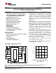
LM3429, LM3429-Q1 SNVS616G – APRIL 2009 – REVISED MAY 2013 www.ti.com Connection Diagram VIN 1 14 HSN COMP 2 13 HSP CSH 3 RCT 4 AGND 5 12 IS DAP 15 11 VCC 10 GATE OVP 6 9 PGND nDIM 7 8 NC Figure 2. 14-Lead TSSOP PIN DESCRIPTIONS Pin Name Description Application Information 1 VIN Input Voltage Bypass with 100 nF capacitor to AGND as close to the device as possible in the circuit board layout. 2 COMP Compensation Connect a capacitor to AGND to set compensation.
LM3429, LM3429-Q1 www.ti.com SNVS616G – APRIL 2009 – REVISED MAY 2013 These devices have limited built-in ESD protection. The leads should be shorted together or the device placed in conductive foam during storage or handling to prevent electrostatic damage to the MOS gates. Absolute Maximum Ratings (1) (2) VIN, nDIM -0.3V to 76.0V -1 mA continuous OVP, HSP, HSN -0.3V to 76.0V -100 µA continuous RCT -0.3V to 3.0V -1 mA to +5 mA continuous IS -0.3V to 76.
LM3429, LM3429-Q1 SNVS616G – APRIL 2009 – REVISED MAY 2013 Electrical Characteristics www.ti.com (1) Specifications in standard type face are for TJ = 25°C and those with boldface type apply over the full Operating Temperature Range ( TJ = −40°C to +125°C). Minimum and Maximum limits are specified through test, design, or statistical correlation. Typical values represent the most likely parametric norm at TJ = +25°C, and are provided for reference purposes only.
LM3429, LM3429-Q1 www.ti.com SNVS616G – APRIL 2009 – REVISED MAY 2013 Electrical Characteristics (1) (continued) Specifications in standard type face are for TJ = 25°C and those with boldface type apply over the full Operating Temperature Range ( TJ = −40°C to +125°C). Minimum and Maximum limits are specified through test, design, or statistical correlation. Typical values represent the most likely parametric norm at TJ = +25°C, and are provided for reference purposes only.
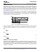
LM3429, LM3429-Q1 SNVS616G – APRIL 2009 – REVISED MAY 2013 www.ti.com Typical Performance Characteristics TA=+25°C and VIN = 14V unless otherwise specified 100 Boost Efficiency vs. Input Voltage VO = 32V (9 LEDs) (1) Buck-Boost Efficiency vs. Input Voltage VO = 20V (6 LEDs) (2) 100 95 EFFICIENCY (%) EFFICIENCY (%) 95 90 90 85 80 85 75 70 80 10 15 20 25 0 30 16 VIN (V) Boost LED Current vs. Input Voltage VO = 32V (9 LEDs) (1) Buck-boost LED Current vs.
LM3429, LM3429-Q1 www.ti.com SNVS616G – APRIL 2009 – REVISED MAY 2013 Typical Performance Characteristics (continued) TA=+25°C and VIN = 14V unless otherwise specified VCSH vs. Junction Temperature VCC vs. Junction Temperature 7.10 1.245 7.05 1.240 7.00 VCC (V) VCSH (V) 1.250 1.235 6.95 1.230 6.90 1.225 6.85 1.220 6.80 -50 -14 22 58 94 130 -50 -14 TEMPERATURE (°C) Figure 9. 58 94 130 Figure 10. VRCT vs. Junction Temperature VLIM vs.
LM3429, LM3429-Q1 SNVS616G – APRIL 2009 – REVISED MAY 2013 www.ti.com BLOCK DIAGRAM VIN 6.9V LDO Regulator UVLO UVLO HYSTERESIS 20 PA nDIM 1.24V VCC VccUVLO Standby REFERENCE 1.24V TLIM Thermal Limit Dimming VIN/25 Reset Dominant Start new on time Q GATE R QB PGND S RCT VCC COMP OVP HYSTERESIS PWM 1.24V CSH 20 PA OVP 1.
LM3429, LM3429-Q1 www.ti.com SNVS616G – APRIL 2009 – REVISED MAY 2013 CURRENT REGULATORS Current regulators can be designed to accomplish three basic functions: buck, boost, and buck-boost. All three topologies in their most basic form contain a main switching MosFET, a recirculating diode, an inductor and capacitors. The LM3429 is designed to drive a ground referenced NFET which is perfect for a standard boost regulator. Buck and buck-boost regulators, on the other hand, usually have a high-side switch.
LM3429, LM3429-Q1 SNVS616G – APRIL 2009 – REVISED MAY 2013 www.ti.com Even though the off-time control is quasi-hysteretic, the input voltage proportionality in the off-timer creates an essentially constant switching frequency over the entire operating range for boost and buck-boost topologies. The buck topology can be designed to give constant ripple over either input voltage or output voltage, however switching frequency is only constant at a specific operating point .
LM3429, LM3429-Q1 www.ti.com SNVS616G – APRIL 2009 – REVISED MAY 2013 VIN RSNS RT LM3429 VIN/25 LED- Start tON RCT CT Reset timer Figure 16. Off-timer Circuitry for Buck Regulators The switching frequency is defined: Buck (Constant Ripple vs. VIN) fSW = 25 x ( VIN - VO ) RT x CT X VIN (4) Buck (Constant Ripple vs.
LM3429, LM3429-Q1 SNVS616G – APRIL 2009 – REVISED MAY 2013 ILED = www.ti.com VSNS 1.24V RHSP x = RSNS RSNS RCSH (9) The selection of the three resistors (RSNS, RCSH, and RHSP) is not arbitrary. For matching and noise performance, the suggested signal current ICSH is approximately 100 µA. This current does not flow in the LEDs and will not affect either the off state LED current or the regulated LED current.
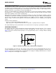
LM3429, LM3429-Q1 www.ti.com IADD = SNVS616G – APRIL 2009 – REVISED MAY 2013 § RADJ x VREF · ¨R + R ¸ - VBE-Q6 © ADJ MAX ¹ RBIAS (10) The corresponding ILED for a specific IADD is: §RHSP· ILED = ICSH - IADD x ¨ ¸ RSNS ( ) © ¹ (11) Variable Current Source LM3429 VCC VREF Q8 Q7 RMAX Q6 RADJ RBIAS CSH RCSH Variable Resistance RADJ Figure 18.
LM3429, LM3429-Q1 SNVS616G – APRIL 2009 – REVISED MAY 2013 www.ti.com There are two possible methods to sense the transistor current. The RDS-ON of the main power MosFET can be used as the current sense resistance because the IS pin was designed to withstand the high voltages present on the drain when the MosFET is in the off state. Alternatively, a sense resistor located in the source of the MosFET may be used for current sensing, however a low inductance (ESL) type is suggested.
LM3429, LM3429-Q1 www.ti.com SNVS616G – APRIL 2009 – REVISED MAY 2013 100 öZ1 80 135 öP1 90 GAIN GAIN (dB) 0 40 PHASE -45 20 0° Phase Margin -90 0 -20 -135 -40 -180 -60 1e-1 PHASE (°) 45 60 1e1 1e3 1e5 -225 1e7 FREQUENCY (Hz) Figure 20. Uncompensated Loop Gain Frequency Response Figure 20 shows the uncompensated loop gain in a worst-case scenario when the RHP zero is below the output pole.
LM3429, LM3429-Q1 SNVS616G – APRIL 2009 – REVISED MAY 2013 ZP2 = www.ti.com 1 5e : x CCMP 6 (17) It may also be necessary to add one final pole at least one decade above the crossover frequency to attenuate switching noise and, in some cases, provide better gain margin. This pole can be placed across RSNS to filter the ESL of the sense resistor at the same time. Figure 21 shows how the compensation is physically implemented in the system.
LM3429, LM3429-Q1 www.ti.com SNVS616G – APRIL 2009 – REVISED MAY 2013 The LM3429 can be configured to detect an output (or input) over-voltage condition via the OVP pin. The pin features a precision 1.24V threshold with 20 µA (typical) of hysteresis current as shown in Figure 23. When the OVLO threshold is exceeded, the GATE pin is immediately pulled low and a 20 µA current source provides hysteresis to the lower threshold of the OVLO hysteretic band.
LM3429, LM3429-Q1 SNVS616G – APRIL 2009 – REVISED MAY 2013 www.ti.com LM3429 VIN 20 PA RUV2 RUV1 nDIM UVLO 1.24V RUVH (optional) Figure 25. UVLO Circuit When using the nDIM pin for UVLO and PWM dimming concurrently, the UVLO circuit can have an extra series resistor to set the hysteresis. This allows the standard resistor divider to have smaller resistor values minimizing PWM delays due to a pull-down MosFET at the nDIM pin (see PWM DIMMING section).
LM3429, LM3429-Q1 www.ti.com SNVS616G – APRIL 2009 – REVISED MAY 2013 Figure 26 shows two ways the PWM signal can be applied to the nDIM pin: 1. Connect the dimming MosFET (QDIM) with the drain to the nDIM pin and the source to GND. Apply an external logic-level PWM signal to the gate of QDIM. A pull down resistor may be necessary to properly turn off QDIM if no signal is present. 2. Connect the anode of a Schottky diode (DDIM) to the nDIM pin.
LM3429, LM3429-Q1 SNVS616G – APRIL 2009 – REVISED MAY 2013 www.ti.com LED DYNAMIC RESISTANCE (rD) When the load is a string of LEDs, the output load resistance is the LED string dynamic resistance plus RSNS. LEDs are PN junction diodes, and their dynamic resistance shifts as their forward current changes. Dividing the forward voltage of a single LED (VLED) by the forward current (ILED) leads to an incorrect calculation of the dynamic resistance of a single LED (rLED).
LM3429, LM3429-Q1 www.ti.com SNVS616G – APRIL 2009 – REVISED MAY 2013 For most applications, it is recommended to bypass the VIN pin with an 0.1 µF ceramic capacitor placed as close as possible to the pin. In situations where the bulk input capacitance may be far from the LM3429 device, a 10Ω series resistor can be placed between the bulk input capacitance and the bypass capacitor, creating a 150 kHz filter to eliminate undesired high frequency noise coupling.
LM3429, LM3429-Q1 SNVS616G – APRIL 2009 – REVISED MAY 2013 www.ti.
LM3429, LM3429-Q1 www.ti.
LM3429, LM3429-Q1 SNVS616G – APRIL 2009 – REVISED MAY 2013 www.ti.com Design Guide Refer to Basic Topology Schematics section.
LM3429, LM3429-Q1 www.ti.com SNVS616G – APRIL 2009 – REVISED MAY 2013 Buck (Constant Ripple vs. VIN) RT = 25 x ( VIN - VO ) fSW x CT X VIN (32) Buck (Constant Ripple vs. VO) 2 RT = 25 x (VIN x VO - VO fSW x C T x ) 2 VIN (33) Boost and Buck-boost 25 RT = fSW x C T (34) 3.
LM3429, LM3429-Q1 SNVS616G – APRIL 2009 – REVISED MAY 2013 www.ti.com Boost and Buck-boost 1 §'IL-PP x D' · x x 1+ IL-RMS = ¸ 12 ¨ ILED D' ILED © 2 ¹ (40) 5. LED RIPPLE CURRENT Set the nominal LED ripple current (ΔiLED-PP), by solving for the output capacitance (CO): Buck CO = 'iL - PP 8 x fSW x rD x 'iLED - PP (41) Boost and Buck-boost ILED x D ü CO = rD x LED - PP x fSW i (42) To set the worst case LED ripple current, use DMAX when solving for CO.
LM3429, LM3429-Q1 www.ti.
LM3429, LM3429-Q1 SNVS616G – APRIL 2009 – REVISED MAY 2013 CCMP = www.ti.com 1 ZP2 x 5e6 (57) If analog dimming is used, CCMP should be approximately 4x larger to maintain stability as the LEDs are dimmed to zero. A high frequency compensation pole (ωP3) can be used to attenuate switching noise and provide better gain margin.
LM3429, LM3429-Q1 www.ti.com SNVS616G – APRIL 2009 – REVISED MAY 2013 Boost ICIN-RMS = 'iL-PP 12 (66) Buck-boost ICIN-RMS = ILED x DMAX 1-DMAX (67) 9.
LM3429, LM3429-Q1 SNVS616G – APRIL 2009 – REVISED MAY 2013 www.ti.com Boost VRD-MAX = VO (77) Buck-boost VRD-MAX = VIN-MAX + VO (78) The current rating should be at least 10% higher than the maximum average diode current (ID-MAX): Buck ID-MAX = (1 - DMIN) x ILED (79) Boost and Buck-boost ID-MAX = ILED (80) Replace DMAX with D in the ID-MAX equation to solve for the average diode current (ID).
LM3429, LM3429-Q1 www.ti.com SNVS616G – APRIL 2009 – REVISED MAY 2013 Method #2: If PWM dimming is required, a three resistor network is suggested. To set VTURN-ON, assume RUV2 = 10 kΩ and solve for RUV1 as in Method #1. To set VHYS, solve for RUVH: RUVH = R UV1 x (VHYS - 20 PA x RUV2) 20 PA x (RUV1 + R UV2) (87) 13. PWM DIMMING METHOD PWM dimming can be performed several ways: Method #1: Connect the dimming MosFET (Q3) with the drain to the nDIM pin and the source to GND.
LM3429, LM3429-Q1 SNVS616G – APRIL 2009 – REVISED MAY 2013 www.ti.com SPECIFICATIONS N=6 VLED = 3.5V rLED = 325 mΩ VIN = 24V VIN-MIN = 10V VIN-MAX = 70V fSW = 700 kHz VSNS = 100 mV ILED = 1A ΔiL-PP = 500 mA ΔiLED-PP = 50 mA ΔvIN-PP = 1V ILIM = 6A VTURN-ON = 10V VHYS = 3V VTURN-OFF = 40V VHYSO = 10V 1. OPERATING POINT Solve for VO and rD: VO = N x VLED = 6 x 3.5V = 21V (88) rD = N x rLED = 6 x 325 m: = 1. 95: (89) Solve for D, D', DMAX, and DMIN: D= VO 21V = = 0.
LM3429, LM3429-Q1 www.ti.com SNVS616G – APRIL 2009 – REVISED MAY 2013 The chosen components from step 2 are: CT = 1 nF RT = 35.7 k: (96) 3. AVERAGE LED CURRENT Solve for RSNS: V 100 mV RSNS = SNS = = 0.1: ILED 1A (97) Assume RCSH = 12.4 kΩ and solve for RHSP: ILED x RCSH x RSNS 1A x 12.4 k : x 0.1: RHSP = = = 1.0 k: 1.24V 1.24V (98) The closest standard resistor for RSNS is actually 0.1Ω and for RHSP is actually 1 kΩ therefore ILED is: 1.24V x RHSP 1.24V x 1.0 k: ILED = = = 1.0A R SNS x R CSH 0.
LM3429, LM3429-Q1 SNVS616G – APRIL 2009 – REVISED MAY 2013 CO = CO = www.ti.com ILED x D rD x 'iLED- PP x fSW 1A x 0. 467 = 6.84 PF 1.95: x 50 mA x 7 00 kHz (105) The closest standard capacitor is 6.8 µF therefore the actual ΔiLED-PP is: I xD 'iLED- PP = LED rD x CO x fSW 'iLED- PP = 1A x 0. 467 = 50 mA 1.95 : x 6.8 PF x 7 00 kHz (106) Determine minimum allowable RMS current rating: ICO- RMS = ILED x DMAX 0.677 = 1.45A = 1A x 1- DMAX 1- 0.677 (107) The chosen components from step 5 are: CO = 6.
LM3429, LM3429-Q1 www.ti.com SNVS616G – APRIL 2009 – REVISED MAY 2013 Solve for CCMP: CCMP = 1 1 = = 0.17 PF ZP2 x 5e6: 1.173 rad x 5e6: sec (116) To attenuate switching noise, calculate ωP3: ZP3 = max ZP1, ZZ1 x 10 = ZP1 x 10 ZP3 = 110 k rad rad x 10 = 1.1M sec sec (117) Assume RFS = 10Ω and solve for CFS: CFS = 1 = 10: x ZP3 1 10: x 1.1M rad sec = 0.091 PF (118) The chosen components from step 7 are: CCOMP = 0.22 PF RFS = 10: CFS = 0.1 PF (119) 8.
LM3429, LM3429-Q1 SNVS616G – APRIL 2009 – REVISED MAY 2013 www.ti.com The chosen component from step 9 is: Q1 o 32A, 100V, DPAK (127) 10. DIODE Determine minimum D1 voltage rating and current rating: VRD - MAX = VIN - MAX + VO = 70V + 21V = 91V (128) ID - MAX = ILED = 1A (129) A 100V diode is chosen with a current rating of 12A and VD = 600 mV. Determine PD: PD = ID x VFD = 1A x 600 mV = 600 mW (130) The chosen component from step 10 is: D1 o 12A, 100V, DPAK (131) 11.
LM3429, LM3429-Q1 www.ti.com SNVS616G – APRIL 2009 – REVISED MAY 2013 R OV1 = 1.24V x ROV2 1.24V x 499 k: = = 15.7 k: VTURN - OFF - 0.62V 40V - 0.62V (139) The closest standard resistor is 15.8 kΩ making VTURN-OFF: VTURN-OFF = VTURN-OFF = 1.24V x (0.5 x ROV1 + ROV2) ROV1 1.24V x (0.5 x 15.8 k: + 499 k:) = 39.8V 15.8 k: (140) The chosen components from step 12 are: ROV1 = 15.
LM3429, LM3429-Q1 SNVS616G – APRIL 2009 – REVISED MAY 2013 www.ti.
LM3429, LM3429-Q1 www.ti.
LM3429, LM3429-Q1 SNVS616G – APRIL 2009 – REVISED MAY 2013 www.ti.
LM3429, LM3429-Q1 www.ti.
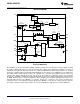
LM3429, LM3429-Q1 SNVS616G – APRIL 2009 – REVISED MAY 2013 www.ti.com DESIGN #6: BUCK APPLICATION - 3 LEDS AT 1.25A 15V ± 50V VIN CIN 1 LM3429 VIN HSN 14 RHSN RT 2 HSP COMP CFS RHSP 13 RSNS CO CCMP RFS 3 CSH IS RCT VCC D1 12 1.
LM3429, LM3429-Q1 www.ti.com SNVS616G – APRIL 2009 – REVISED MAY 2013 DESIGN #7: BUCK-BOOST THERMAL FOLDBACK APPLICATION - 8 LEDs at 2.5A L1 15V ± 60V VIN VREF D1 CIN RT 1 RGAIN CCMP RNTC 2 VIN LM3429 HSN HSP COMP 14 RHSN 13 RHSP 2.
LM3429, LM3429-Q1 SNVS616G – APRIL 2009 – REVISED MAY 2013 www.ti.
LM3429, LM3429-Q1 www.ti.com SNVS616G – APRIL 2009 – REVISED MAY 2013 REVISION HISTORY Changes from Revision F (May 2013) to Revision G • Page Changed layout of National Data Sheet to TI format ..........................................................................................................
PACKAGE OPTION ADDENDUM www.ti.
PACKAGE OPTION ADDENDUM www.ti.
PACKAGE MATERIALS INFORMATION www.ti.com 8-May-2013 TAPE AND REEL INFORMATION *All dimensions are nominal Device Package Package Pins Type Drawing SPQ Reel Reel A0 Diameter Width (mm) (mm) W1 (mm) LM3429MHX/NOPB HTSSOP PWP 14 2500 330.0 12.4 LM3429Q1MHX/NOPB HTSSOP PWP 14 2500 330.0 12.4 Pack Materials-Page 1 B0 (mm) K0 (mm) P1 (mm) W Pin1 (mm) Quadrant 6.95 8.3 1.6 8.0 12.0 Q1 6.95 8.3 1.6 8.0 12.
PACKAGE MATERIALS INFORMATION www.ti.com 8-May-2013 *All dimensions are nominal Device Package Type Package Drawing Pins SPQ Length (mm) Width (mm) Height (mm) LM3429MHX/NOPB HTSSOP PWP 14 2500 367.0 367.0 35.0 LM3429Q1MHX/NOPB HTSSOP PWP 14 2500 367.0 367.0 35.
MECHANICAL DATA PWP0014A MXA14A (Rev A) www.ti.
IMPORTANT NOTICE Texas Instruments Incorporated and its subsidiaries (TI) reserve the right to make corrections, enhancements, improvements and other changes to its semiconductor products and services per JESD46, latest issue, and to discontinue any product or service per JESD48, latest issue. Buyers should obtain the latest relevant information before placing orders and should verify that such information is current and complete.