
Datasheet

V
SNS
= 1.24V x
R
CSH
R
HSP
I
CSH
=
R
HSP
V
SNS
TT
SW
CR
25
f
x
=
( )
2
OOIN
VVV25 -
xx
SW
f
=
2
INTT
VCR
xx
f
SW
=
25 x V
IN
- V
O
R
T
x C
T
X V
IN
( )
R
T
C
T
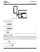
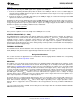
LM3429
RCT
Start t
ON
V
IN
/25
Reset timer
R
SNS
V
IN
LED-
LM3429, LM3429-Q1
www.ti.com
SNVS616G –APRIL 2009–REVISED MAY 2013
Figure 16. Off-timer Circuitry for Buck Regulators
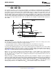
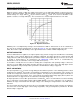
The switching frequency is defined:
Buck (Constant Ripple vs. V
IN
)
(4)
Buck (Constant Ripple vs. V
O
)
(5)
Boost and Buck-boost
(6)
For all topologies, the C
T
capacitor is recommended to be 1 nF and should be located very close to the LM3429.
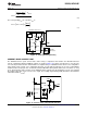
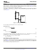
AVERAGE LED CURRENT
The LM3429 uses an external current sense resistor (R
SNS
) placed in series with the LED load to convert the
LED current (I
LED
) into a voltage (V
SNS
) as shown in Figure 17. The HSP and HSN pins are the inputs to the
high-side sense amplifier which are forced to be equal potential (V
HSP
=V
HSN
) through negative feedback.
Because of this, the V
SNS
voltage is forced across R
HSP
to generate the signal current (I
CSH
) which flows out of
the CSH pin and through the R
CSH
resistor. The error amplifier will regulate the CSH pin to 1.24V, therefore I
CSH
can be calculated:
(7)
This means V
SNS
will be regulated as follows:
(8)
I
LED
can then be calculated:
Copyright © 2009–2013, Texas Instruments Incorporated Submit Documentation Feedback 11
Product Folder Links: LM3429 LM3429-Q1