
Datasheet

R
SNS
I
LED
R
HSP
R
HSN
HSN
HSP
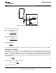
High-Side
Sense Amplifier
CSH
1.24V
C
CMP
R
CSH
COMP
Error Amplifier
V
SNS
To PWM
Comparator
LM3429
I
CSH
I
LED
=
R
SNS
1.24V
R
SNS
V
SNS
R
CSH
R
HSP
=
x
LM3429, LM3429-Q1
SNVS616G –APRIL 2009–REVISED MAY 2013
www.ti.com
(9)
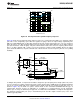
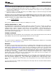
The selection of the three resistors (R
SNS
, R
CSH
, and R
HSP
) is not arbitrary. For matching and noise performance,
the suggested signal current I
CSH
is approximately 100 µA. This current does not flow in the LEDs and will not
affect either the off state LED current or the regulated LED current. I
CSH
can be above or below this value, but
the high-side amplifier offset characteristics may be affected slightly. In addition, to minimize the effect of the
high-side amplifier voltage offset on LED current accuracy, the minimum V
SNS
is suggested to be 50 mV. Finally,
a resistor (R
HSN
= R
HSP
) should be placed in series with the HSN pin to cancel out the effects of the input bias
current (~10 µA) of both inputs of the high-side sense amplifier. Note that he CSH pin can also be used as a low-
side current sense input regulated to the 1.24V. The high-side sense amplifier is disabled if HSP and HSN are
tied to GND.
Figure 17. LED Current Sense Circuitry
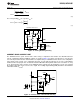
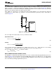
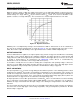
ANALOG DIMMING
The CSH pin can be used to analog dim the LED current by adjusting the current sense voltage (V
SNS
). There
are several different methods to adjust V
SNS
using the CSH pin:
1. External variable resistance : Adjust a potentiometer placed in series with R
CSH
to vary V
SNS
.
2. External variable current source: Source current (0 µA to I
CSH
) into the CSH pin to adjust V
SNS
.
In general, analog dimming applications require a lower switching frequency to minimize the effect of the leading
edge blanking circuit. As the LED current is reduced, the output voltage and the duty cycle decreases.
Eventually, the minimum on-time is reached. The lower the switching frequency, the wider the linear dimming
range. Figure 18 shows how both methods are physically implemented.
Method 1 uses an external potentiometer in the CSH path which is a simple addition to the existing circuitry.
However, the LEDs cannot dim completely because there is always some resistance causing signal current to
flow. This method is also susceptible to noise coupling at the CSH pin since the potentiometer increases the size
of the signal current loop.
Method 2 provides a complete dimming range and better noise performance, though it is more complex. It
consists of a PNP current mirror and a bias network consisting of an NPN, 2 resistors and a potentiometer
(R
ADJ
), where R
ADJ
controls the amount of current sourced into the CSH pin. A higher resistance value will source
more current into the CSH pin causing less regulated signal current through R
HSP
, effectively dimming the LEDs.
V
REF
should be a precise external voltage reference, while Q7 and Q8 should be a dual pair PNP for best
matching and performance. The additional current (I
ADD
) sourced into the CSH pin can be calculated:
12 Submit Documentation Feedback Copyright © 2009–2013, Texas Instruments Incorporated
Product Folder Links: LM3429 LM3429-Q1