
Datasheet
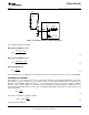
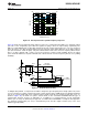

R
SNS
I
LED
R
HSP
R
HSN
HSN
HSP
High-Side
Sense Amplifier
CSH
1.24V
C
CMP
R
CSH
COMP
Error Amplifier
V
SNS
To PWM
Comparator
LM3429
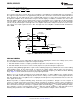
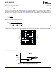
C
FS
R
FS
sets ö
P3
R
O
sets ö
P2
PHASE (°)
FREQUENCY (Hz)
GAIN (dB)
100
80
60
40
20
0
-20
-40
-60
135
90
45
0
-45
-90
-135
-180
-225
1e-1 1e1 1e3 1e5 1e7
0° Phase Margin
ö
P1
PHASE
GAIN
ö
Z1
LM3429, LM3429-Q1
www.ti.com
SNVS616G –APRIL 2009–REVISED MAY 2013
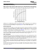
Figure 20. Uncompensated Loop Gain Frequency Response
Figure 20 shows the uncompensated loop gain in a worst-case scenario when the RHP zero is below the output
pole. This occurs at high duty cycles when the regulator is trying to boost the output voltage significantly. The
RHP zero adds 20dB/decade of gain while loosing 45°/decade of phase which places the crossover frequency
(when the gain is zero dB) extremely high because the gain only starts falling again due to the high frequency
pole (not modeled or shown in figure). The phase will be below -180° at the crossover frequency which means
there is no phase margin (180° + phase at crossover frequency) causing system instability. Even if the output
pole is below the RHP zero, the phase will still reach -180° before the crossover frequency in most cases yielding
instability.
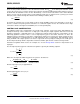
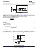
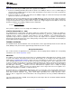
Figure 21. Compensation Circuitry
To mitigate this problem, a compensator should be designed to give adequate phase margin (above 45°) at the
crossover frequency. A simple compensator using a single capacitor at the COMP pin (C
CMP
) will add a dominant
pole to the system, which will ensure adequate phase margin if placed low enough. At high duty cycles (as
shown in Figure 20), the RHP zero places extreme limits on the achievable bandwidth with this type of
compensation. However, because an LED driver is essentially free of output transients (except catastrophic
failures open or short), the dominant pole approach, even with reduced bandwidth, is usually the best approach.
The dominant compensation pole (ω
P2
) is determined by C
CMP
and the output resistance (R
O
) of the error
amplifier (typically 5 MΩ):
Copyright © 2009–2013, Texas Instruments Incorporated Submit Documentation Feedback 15
Product Folder Links: LM3429 LM3429-Q1