
Datasheet

1.24V
20 PA
LM3429
R
OV2
R
OV1
V
O
OVLO
OVP
PHASE (°)
FREQUENCY (Hz)
GAIN (dB)
80
60
40
20
0
-20
-40
-60
-80
90
45
0
-45
-90
-135
-180
-225
-270
1e-1 1e1 1e3 1e5 1e7
GAIN
60° Phase Margin
PHASE
ö
P2
ö
P3
ö
P1
ö
Z1
x=
0U
TT
-1
¸
¸
¹
·
¨
¨
©
§
s
Z
1
Z
xx +1
¸
¸
¹
·
¨
¨
©
§
s
Z
3P
+1
¸
¸
¹
·
¨
¨
©
§
s
Z
2P
+1
¸
¸
¹
·
¨
¨
©
§
s
Z
1P
1
3P
=Z
FSFS
CR x
1
2P
=Z
CMP
6
Ce5 x
:
LM3429, LM3429-Q1
SNVS616G –APRIL 2009–REVISED MAY 2013
www.ti.com
(17)
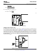
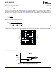
It may also be necessary to add one final pole at least one decade above the crossover frequency to attenuate
switching noise and, in some cases, provide better gain margin. This pole can be placed across R
SNS
to filter the
ESL of the sense resistor at the same time. Figure 21 shows how the compensation is physically implemented in
the system.
The high frequency pole (ω
P3
) can be calculated:
(18)
The total system transfer function becomes:
(19)
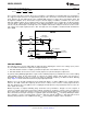
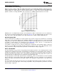
The resulting compensated loop gain frequency response shown in Figure 22 indicates that the system has
adequate phase margin (above 45°) if the dominant compensation pole is placed low enough, ensuring stability:
Figure 22. Compensated Loop Gain Frequency Response
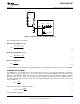
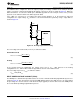
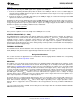
OUTPUT OVER-VOLTAGE LOCKOUT (OVLO)
Figure 23. Over-Voltage Protection Circuitry
16 Submit Documentation Feedback Copyright © 2009–2013, Texas Instruments Incorporated
Product Folder Links: LM3429 LM3429-Q1