
Datasheet

V
IN
nDIM
AGND
OVP
CSH
RCT
GATE
1
COMP HSP
DAP
IS
2
3
4
5
6
7
14
13
12
11
10
9
8
NC
PGND
HSN
V
CC
15
LM3429, LM3429-Q1
SNVS616G –APRIL 2009–REVISED MAY 2013
www.ti.com
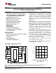
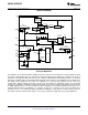
Connection Diagram
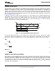
Figure 2. 14-Lead TSSOP
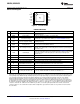
PIN DESCRIPTIONS
Pin Name Description Application Information
Bypass with 100 nF capacitor to AGND as close to the device as possible in the
1 V
IN
Input Voltage
circuit board layout.
2 COMP Compensation Connect a capacitor to AGND to set compensation.
Connect a resistor to AGND to set signal current. For analog dimming, connect
3 CSH Current Sense High
current source or potentiometer to AGND (see ANALOG DIMMING section).
Connect a resistor from the switch node and a capacitor to AGND to set the
4 RCT Resistor Capacitor Timing
switching frequency.
Connect to PGND through the DAP copper circuit board pad to provide proper
5 AGND Analog Ground
ground return for CSH, COMP, and RCT.
Connect to a resistor divider from V
O
to program output over-voltage lockout
6 OVP Over-Voltage Protection (OVLO). Turn-off threshold is 1.24V and hysteresis for turn-on is provided by 20
µA current source.
Connect a PWM signal for dimming as detailed in the PWM DIMMING section
and/or a resistor divider from V
IN
to program input under-voltage lockout (UVLO).
7 nDIM Not DIM input
Turn-on threshold is 1.24V and hysteresis for turn-off is provided by 20 µA
current source.
8 NC No Connection Leave open.
9 PGND Power Ground Connect to AGND through DAP copper pad to provide ground return for GATE.
10 GATE Gate Drive Output Connect to the gate of the external NFET.
11 V
CC
Internal Regulator Output Bypass with a 2.2 µF–3.3 µF, ceramic capacitor to PGND.
Connect to the drain of the main N-channel MosFET switch for R
DS-ON
sensing or
12 IS Main Switch Current Sense
to a sense resistor installed in the source of the same device.
13 HSP LED Current Sense Positive Connect through a series resistor to LED current sense resistor (positive).
14 HSN LED Current Sense Negative Connect through a series resistor to LED current sense resistor (negative).
DA
P DAP Thermal pad on bottom of IC Connect to AGND and PGND. For thermal considerations see
(1)
.
(15)
(1) Junction-to-ambient thermal resistance is highly board-layout dependent. The numbers listed in the table are given for a reference layout
wherein the 14L TSSOP package has its DAP pad populated with 9 vias. In applications where high maximum power dissipation exists,
namely driving a large MosFET at high switching frequency from a high input voltage, special care must be paid to thermal dissipation
issues during board design. In high-power dissipation applications, the maximum ambient temperature may have to be derated.
Maximum ambient temperature (T
A-MAX
) is dependent on the maximum operating junction temperature (T
J-MAX-OP
= 125°C), the
maximum power dissipation of the device in the application (P
D-MAX
), and the junction-to ambient thermal resistance of the package in
the application (θ
JA
), as given by the following equation: T
A-MAX
= T
J-MAX-OP
– (θ
JA
× P
D-MAX
). In most applications there is little need for
the full power dissipation capability of this advanced package. Under these circumstances, no vias would be required and the thermal
resistances would be 104 °C/W for the 14L TSSOP. It is possible to conservatively interpolate between the full via count thermal
resistance and the no via count thermal resistance with a straight line to get a thermal resistance for any number of vias in between
these two limits.
2 Submit Documentation Feedback Copyright © 2009–2013, Texas Instruments Incorporated
Product Folder Links: LM3429 LM3429-Q1