
Datasheet

R
UV1
=
1.24VV
ONTURN
-
-
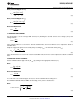
R1.24V
UV2
x
R
UV2
=
A20 P
V
HYS
R
OV1
=
R1.24V
OV2
x
Vm620V
OFFTURN
-
-
R
OV1
=
1.24VV
OFFTURN
-
-
R1.24V
OV2
x
R
OV2
=
V
HYSO
A20P
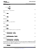
FDDD
VIP
x=
I
D-MAX
= I
LED
I
D-MAX
= (1 - D
MIN
) x I
LED
V
RD-MAX
= V
IN-MAX
+ V
O
V
RD-MAX
= V
O
LM3429, LM3429-Q1
SNVS616G –APRIL 2009–REVISED MAY 2013
www.ti.com
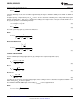
Boost
(77)
Buck-boost
(78)
The current rating should be at least 10% higher than the maximum average diode current (I
D-MAX
):
Buck
(79)
Boost and Buck-boost
(80)
Replace D
MAX
with D in the I
D-MAX
equation to solve for the average diode current (I
D
). Given a diode with forward
voltage (V
FD
), solve for the nominal power dissipation (P
D
):
(81)
11. OUTPUT OVLO
For boost and buck-boost regulators, output OVLO is programmed with the turn-off threshold voltage (V
TURN-OFF
)
and the desired hysteresis (V
HYSO
). To set V
HYSO
, solve for R
OV2
:
(82)
To set V
TURN-OFF
, solve for R
OV1
:
Boost
(83)
Buck-boost
(84)
A small filter capacitor (C
OVP
= 47 pF) should be added from the OVP pin to ground to reduce coupled switching
noise.
12. INPUT UVLO
For all topologies, input UVLO is programmed with the turn-on threshold voltage (V
TURN-ON
) and the desired
hysteresis (V
HYS
).
Method #1: If no PWM dimming is required, a two resistor network can be used. To set V
HYS
, solve for R
UV2
:
(85)
To set V
TURN-ON
, solve for R
UV1
:
(86)
30 Submit Documentation Feedback Copyright © 2009–2013, Texas Instruments Incorporated
Product Folder Links: LM3429 LM3429-Q1