
Datasheet

D1
OVP
LM3429
nDIM
PGND
NC
DAP
GATE
COMP
CSH
RCT
IS
HSN
HSP
L1
C
IN
C
BYP
Q1
C
CMP
R
CSH
C
T
R
UV2
R
UV1
1
2
3
4
5
6
7
14
13
12
11
10
9
8
R
HSN
R
HSP
1A
C
O
R
SNS
AGND
R
T
R
FS
C
FS
I
LED
Q2
R
OV2
R
OV1
C
OV
V
IN
V
IN
V
IN
10V ± 70V
V
IN
V
CC
R
LIM
( )
RR +x
2UV1UV
A20P
( )
x
HYS
A20V xP- R
2UV
R
1UV
UVH
R =
LM3429, LM3429-Q1
www.ti.com
SNVS616G –APRIL 2009–REVISED MAY 2013
Method #2: If PWM dimming is required, a three resistor network is suggested. To set V
TURN-ON
, assume R
UV2
=
10 kΩ and solve for R
UV1
as in Method #1. To set V
HYS
, solve for R
UVH
:
(87)
13. PWM DIMMING METHOD
PWM dimming can be performed several ways:
Method #1: Connect the dimming MosFET (Q
3
) with the drain to the nDIM pin and the source to GND. Apply an
external PWM signal to the gate of Q
DIM
. A pull down resistor may be necessary to properly turn off Q
3
.
Method #2: Connect the anode of a Schottky diode to the nDIM pin. Apply an external inverted PWM signal to
the cathode of the same diode.
14. ANALOG DIMMING METHOD
Analog dimming can be performed several ways:
Method #1: Place a potentiometer in series with the R
CSH
resistor to dim the LED current from the nominal I
LED
to near zero.
Method #2: Connect a controlled current source as detailed in the ANALOG DIMMING section to the CSH pin.
Increasing the current sourced into the CSH node will decrease the LEDs from the nominal I
LED
to zero current.
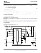
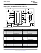
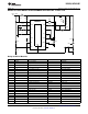
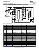
Design Example #1
BUCK-BOOST APPLICATION - 6 LEDs at 1A
Copyright © 2009–2013, Texas Instruments Incorporated Submit Documentation Feedback 31
Product Folder Links: LM3429 LM3429-Q1