
Datasheet

LM3429, LM3429-Q1
SNVS616G –APRIL 2009–REVISED MAY 2013
www.ti.com
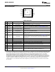
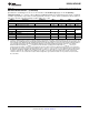
Electrical Characteristics
(1)
Specifications in standard type face are for T
J
= 25°C and those with boldface type apply over the full Operating
Temperature Range ( T
J
= −40°C to +125°C). Minimum and Maximum limits are specified through test, design, or statistical
correlation. Typical values represent the most likely parametric norm at T
J
= +25°C, and are provided for reference purposes
only. Unless otherwise stated the following condition applies: V
IN
= +14V.
Symbol Parameter Conditions Min
(2)
Typ
(3)
Max
(2)
Units
STARTUP REGULATOR (V
CC
)
V
CC-REG
V
CC
Regulation I
CC
= 0 mA 6.30 6.90 7.35 V
I
CC-LIM
V
CC
Current Limit V
CC
= 0V 20 27
mA
I
Q
Quiescent Current Static 1.6 3.0
V
CC-UVLO
V
CC
UVLO Threshold V
CC
Increasing 4.17 4.50
V
CC
Decreasing 3.70 4.08 V
V
CC-HYS
V
CC
UVLO Hysteresis 0.1
OVER-VOLTAGE PROTECTION (OVP)
V
TH-OVP
OVP OVLO Threshold OVP Increasing 1.180 1.240 1.280 V
I
HYS-OVP
OVP Hysteresis Source Current OVP Active (high) 10 20 30 µA
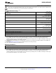
ERROR AMPLIFIER
V
CSH
CSH Reference Voltage With Respect to AGND 1.210 1.235 1.260 V
Error Amplifier Input Bias Current -0.6 0 0.6
µA
COMP Sink / Source Current 10 26 40
Transconductance 100 µA/V
Linear Input Range
(4)
±125 mV
Transconductance Bandwidth -6dB Unloaded
0.5 1.0 MHz
Response
(4)
OFF TIMER (RCT)
t
OFF-MIN
Minimum Off-time RCT = 1V through 1 kΩ 35 75 ns
R
RCT
RCT Reset Pull-down Resistance 36 120 Ω
V
RCT
V
IN
/25 Reference Voltage V
IN
= 14V 540 565 585 mV
PWM COMPARATOR
COMP to PWM Offset 700 800 900 mV
CURRENT LIMIT (IS)
V
LIM
Current Limit Threshold 215 245 275 mV
V
LIM
Delay to Output 35 75
ns
t
ON-MIN
Leading Edge Blanking Time 75 250 450
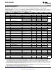
HIGH SIDE TRANSCONDUCTANCE AMPLIFIER
Input Bias Current 10 µA
Transconductance 20 119 mA/V
Input Offset Current -1.5 0 1.5 µA
Input Offset Voltage -7 0 7 mV
Transconductance Bandwidth I
CSH
= 100 µA
(4)
250 500 kHz
GATE DRIVER (GATE)
R
SRC(GATE)
GATE Sourcing Resistance GATE = High 2.0 6.0
Ω
R
SNK(GATE)
GATE Sinking Resistance GATE = Low 1.3 4.5
(1) Absolute Maximum Ratings indicate limits beyond which damage to the device may occur, including inoperability and degradation of
device reliability and/or performance. Functional operation of the device and/or non-degradation at the Absolute Maximum Ratings or
other conditions beyond those indicated in the Operating Ratings is not implied. The recommended Operating Ratings indicate
conditions at which the device is functional and the device should not be operated beyond such conditions. All voltages are with respect
to the potential at the AGND pin, unless otherwise specified.
(2) All limits specified at room temperature (standard typeface) and at temperature extremes (bold typeface). All room temperature limits are
100% production tested. All limits at temperature extremes are specified via correlation using standard Statistical Quality Control (SQC)
methods. All limits are used to calculate Average Outgoing Quality Level (AOQL).
(3) Typical numbers are at 25°C and represent the most likely norm.
(4) These electrical parameters are specified by design, and are not verified by test.
4 Submit Documentation Feedback Copyright © 2009–2013, Texas Instruments Incorporated
Product Folder Links: LM3429 LM3429-Q1