
Datasheet

1
4
3
2
10
7
8
9
I
SNS
NC
GATE
NC
COFF
V
CC
NC
NC
5 6FILTER GND
3
2
1
6
7
8
VCC
NC
NC
GND
COFF
FILTER
4 5
I
SNS
GATE
LM3444
SNVS682C –NOVEMBER 2010–REVISED MAY 2013
www.ti.com
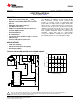
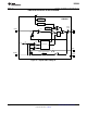
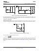
Connection Diagrams
Figure 1. 10-Pin VSSOP (Top View) Figure 2. 8-Lead SOIC (Top View)
See DGS Package See D Package
PIN DESCRIPTIONS
VSSOP SOIC Name Description
1 1 NC No internal connection. Leave this pin open.
2 NC No internal connection. Leave this pin open.
3 NC No internal connection. Leave this pin open.
4 8 COFF OFF time setting pin. A user set current and capacitor connected from the output to this pin sets the
constant OFF time of the switching controller.
5 2 FILTER Filter input. A low pass filter tied to this pin can filter a PWM dimming signal to supply a DC voltage to
control the LED current. Can also be used as an analog dimming input. If not used for dimming connect a
0.1µF capacitor from this pin to ground.
6 3 GND Circuit ground connection.
7 4 ISNS LED current sense pin. Connect a resistor from main switching MOSFET source, ISNS to GND to set the
maximum LED current.
8 5 GATE Power MOSFET driver pin. This output provides the gate drive for the power switching MOSFET of the
buck controller.
9 6 V
CC
Input voltage pin. This pin provides the power for the internal control circuitry and gate driver.
10 7 NC No internal connection. Leave this pin open.
2 Submit Documentation Feedback Copyright © 2010–2013, Texas Instruments Incorporated
Product Folder Links: LM3444