
Datasheet

LM3691
SNVS506I –MAY 2008–REVISED MAY 2013
www.ti.com
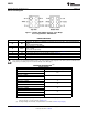
Electrical Characteristics
(1) (2) (3)
Limits in standard typeface are for T
A
= 25°C. Limits in boldface type apply over the operating ambient temperature range
(−30°C ≤ T
A
= T
J
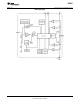
≤ +85°C). Unless otherwise noted, specifications apply to the LM3691 open loop Typical Application Circuit
with V
IN
= EN = 3.6V.
Parameter Test Conditions Min Typ Max Units
V
FB
Feedback Voltage PWM Mode. No load V
OUT
= 1.1V to 3.3V -1 +1 %
PWM Mode. No load V
OUT
= 0.75V to 1.0V -10 +10 mV
I
SHDN
Shutdown Supply Current EN = 0V 0.03 1 µA
I
Q_ECO
ECO Mode I
q
ECO Mode 64 80 µA
I
Q_PWM
PWM Mode I
q
PWM Mode 490 600 µA
R
DSON (P)
Pin-Pin Resistance for PFET V
IN
= V
GS
= 3.6V, I
O
= 200 mA 160 250 mΩ
R
DSON (N)
Pin-Pin Resistance for NFET V
IN
= V
GS
= 3.6V, I
O
= −200 mA 115 180 mΩ
I
LIM
Switch Peak Current Limit Open loop 1250 1500 1700 mA
V
IH
Logic High Input 1.2 V
V
IL
Logic Low Input 0.4 V
I
EN,MODE
Input Current 0.01 1 µA
F
SW
Switching Frequency PWM Mode 3.6 4 4.4 MHz
V
ON
UVLO threshold
(4)
V
IN
rising 2.2 2.29 V
V
IN
falling 2.1 V
T
STARTUP
Start Time
(5)
70 145 300 µs
(1) All voltages are with respect to the potential at the GND pin.
(2) Min and Max limits are specified by design, test or statistical analysis. Typical numbers represent the most likely norm.
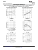
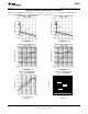
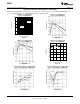
(3) The parameters in the electrical characteristic table are tested under open loop conditions at V
IN
= 3.6V unless otherwise specified. For
performance over the input voltage range and closed loop condition, refer to the datasheet curves.
(4) The UVLO rising threshold minus the falling threshold is always positive.
(5) Specified by design. Not production tested.
4 Submit Documentation Feedback Copyright © 2008–2013, Texas Instruments Incorporated
Product Folder Links: LM3691