
Datasheet


Register 12: GPIO 4-mA Drive Select (GPIODR4R), offset 0x504
The GPIODR4R register is the 4-mA drive control register. It allows for each GPIO signal in the port
to be individually configured without affecting the other pads. When writing the DRV4 bit for a GPIO
signal, the corresponding DRV2 bit in the GPIODR2R register and the DRV8 bit in the GPIODR8R
register are automatically cleared by hardware.
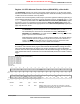
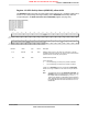
GPIO 4-mA Drive Select (GPIODR4R)
GPIO Port A base: 0x4000.4000
GPIO Port B base: 0x4000.5000
GPIO Port C base: 0x4000.6000
GPIO Port D base: 0x4000.7000
GPIO Port E base: 0x4002.4000
GPIO Port F base: 0x4002.5000
GPIO Port G base: 0x4002.6000
Offset 0x504
Type R/W, reset 0x0000.0000
16171819202122232425262728293031
reserved
ROROROROROROROROROROROROROROROROType
0000000000000000Reset
0123456789101112131415
DRV4reserved
R/WR/WR/WR/WR/WR/WR/WR/WROROROROROROROROType
0000000000000000Reset
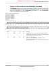
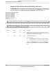
DescriptionResetTypeNameBit/Field
Software should not rely on the value of a reserved bit. To provide
compatibility with future products, the value of a reserved bit should be
preserved across a read-modify-write operation.
0x00ROreserved31:8
Output Pad 4-mA Drive Enable
A write of 1 to either GPIODR2[n] or GPIODR8[n] clears the
corresponding 4-mA enable bit. The change is effective on the second
clock cycle after the write.
0x00R/WDRV47:0
June 18, 2012314
Texas Instruments-Production Data
General-Purpose Input/Outputs (GPIOs)
NRND: Not recommended for new designs.