
Datasheet
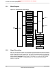

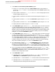
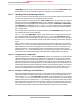

15.1 Block Diagram
Figure 15-1. CAN Controller Block Diagram
CAN Control
CAN Core
Message Object
Registers
CANNWDA2
CANMSG1INT
CANMSG2INT
CANMSG1VAL
CANMSG2VAL
CAN Tx
CANINT
CANTST
CANBRPE
CANBIT
APB
Interface
ABP
Pins
Message RAM
32 Message Objects
CANERR
CANCTL
CANSTS
CANIF2ARB2
CANIF2MCTL
CANIF2DA1
CAN Interface 2
CANIF2DA2
CANIF2DB1
CANIF2DB2
CANIF2ARB1
CANIF2MSK2
CANIF2CRQ
CANIF2CMSK
CANIF2MSK1
CAN Interface 1
CANIF1CRQ
CANIF1CMSK
CANIF1MSK1
CANIF1MSK2
CANIF1ARB1
CANIF1ARB2
CANIF1MCTL
CANIF1DA1
CANIF1DA2
CANIF1DB1
CANIF1DB2
CAN Rx
CANNWDA1
CANTXRQ1
CANTXRQ2
15.2 Signal Description
Table 15-1 on page 553 and Table 15-2 on page 553 list the external signals of the CAN controller
and describe the function of each. The CAN controller signals are alternate functions for some GPIO
signals and default to be GPIO signals at reset. The column in the table below titled "Pin Assignment"
lists the possible GPIO pin placements for the CAN signals. The AFSEL bit in the GPIO Alternate
Function Select (GPIOAFSEL) register (page 311) should be set to choose the CAN controller
function. For more information on configuring GPIOs, see “General-Purpose Input/Outputs
(GPIOs)” on page 289.
June 18, 2012552
Texas Instruments-Production Data
Controller Area Network (CAN) Module
NRND: Not recommended for new designs.