
Datasheet
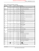
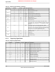
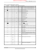
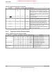
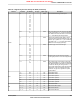
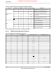

Table 21-2. Signals by Signal Name (continued)
DescriptionBuffer Type
a
Pin TypePin NumberPin Name
The positive supply for the analog circuits (ADC, Analog
Comparators, etc.). These are separated from VDD to
minimize the electrical noise contained on VDD from affecting
the analog functions. VDDA pins must be supplied with a
voltage that meets the specification in “Recommended DC
Operating Conditions” on page 748, regardless of system
implementation.
Power-3
98
VDDA
An external input that brings the processor out of Hibernate
mode when asserted.
TTLI50WAKE
Hibernation module oscillator crystal input or an external clock
reference input. Note that this is either a crystal or a
32.768-kHz oscillator for the Hibernation module RTC.
AnalogI52XOSC0
Hibernation module oscillator crystal output. Leave
unconnected when using a single-ended clock source.
AnalogO53XOSC1
Ethernet PHY XTALN 25-MHz oscillator crystal output.
Connect this pin to ground when using a single-ended 25-MHz
clock input connected to the XTALPPHY pin.
TTLO17XTALNPHY
Ethernet PHY XTALP 25-MHz oscillator crystal input or
external clock reference input.
TTLI16XTALPPHY
a. The TTL designation indicates the pin has TTL-compatible voltage levels.
21.1.3 Signals by Function, Except for GPIO
Table 21-3. Signals by Function, Except for GPIO
DescriptionBuffer Type
a
Pin TypePin NumberPin NameFunction
Analog-to-digital converter input 0.AnalogI1ADC0
ADC
Analog-to-digital converter input 1.AnalogI2ADC1
Analog-to-digital converter input 2.AnalogI5ADC2
Analog-to-digital converter input 3.AnalogI6ADC3
Analog comparator 0 positive input.AnalogI90C0+
Analog Comparators
Analog comparator 0 negative input.AnalogI92C0-
Analog comparator 0 output.TTLO91C0o
CAN module 0 receive.TTLI10CAN0Rx
Controller Area
Network
CAN module 0 transmit.TTLO11CAN0Tx
June 18, 2012726
Texas Instruments-Production Data
Signal Tables
NRND: Not recommended for new designs.