
Datasheet
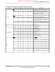
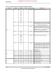
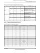
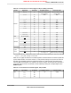
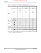
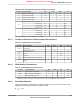
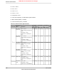

Table 21-7. Signals by Function, Except for GPIO (continued)
DescriptionBuffer Type
a
Pin TypePin NumberPin NameFunction
CPU Mode bit 0. Input must be set to logic 0
(grounded); other encodings reserved.
TTLIE11CMOD0
System Control &
Clocks
CPU Mode bit 1. Input must be set to logic 0
(grounded); other encodings reserved.
TTLIB10CMOD1
Main oscillator crystal input or an external clock
reference input.
AnalogIL11OSC0
Main oscillator crystal output. Leave unconnected
when using a single-ended clock source.
AnalogOM11OSC1
System reset input.TTLIH11RST
UART module 0 receive. When in IrDA mode, this
signal has IrDA modulation.
TTLIL3U0Rx
UART
UART module 0 transmit. When in IrDA mode, this
signal has IrDA modulation.
TTLOM3U0Tx
UART module 1 receive. When in IrDA mode, this
signal has IrDA modulation.
TTLIH2U1Rx
UART module 1 transmit. When in IrDA mode, this
signal has IrDA modulation.
TTLOH1U1Tx
a. The TTL designation indicates the pin has TTL-compatible voltage levels.
21.2.4 GPIO Pins and Alternate Functions
Table 21-8. GPIO Pins and Alternate Functions
Multiplexed FunctionMultiplexed FunctionPin NumberIO
U0RxL3PA0
U0TxM3PA1
SSI0ClkM4PA2
SSI0FssL4PA3
SSI0RxL5PA4
SSI0TxM5PA5
CCP1L6PA6
M6PA7
PWM2E12PB0
PWM3D12PB1
I2C0SCLC11PB2
I2C0SDAC12PB3
C0-A6PB4
C0oB7PB5
C0+A7PB6
TRSTA8PB7
SWCLKTCKA9PC0
SWDIOTMSB9PC1
TDIB8PC2
SWOTDOA10PC3
PhA0L1PC4
743June 18, 2012
Texas Instruments-Production Data
Stellaris
®
LM3S8962 Microcontroller
NRND: Not recommended for new designs.