
Datasheet

LM5033
SNVS181B –APRIL 2004–REVISED APRIL 2013
www.ti.com
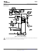
FUNCTIONAL DESCRIPTION
The LM5033 High Voltage PWM controller contains all of the features needed to implement Push-Pull and Bridge
topologies, using voltage-mode control in a small 10 pin package. Features included are: startup regulator,
precision 2.5V reference output, current limit detection, alternating gate drivers, sync capability, thermal
shutdown, softstart, and remote shutdown. This high speed IC has total propagation delays <100 ns. These
features simplify the design of an open loop DC-DC converter, or a voltage controlled closed loop converter. The
Functional Block Diagram is shown in Figure 2.
High Voltage Start-Up Regulator (Pins 1, 4)
The LM5033 contains an internal high voltage startup regulator. The input pin (V
IN
) can be connected directly to
line voltages as high as 90V for normal operation, and can withstand transients to 100V. The regulator output at
V
CC
(9.6V) is internally current limited and sources a minimum of 20mA. Upon power up, the capacitor at V
CC
will
charge up, providing a time delay while internal circuits stabilize. When V
CC
reaches the upper threshold of the
under-voltage sensor (typically 9.5V), the under-voltage sensor resets, enabling the output drivers, although the
PWM duty cycle will initially be at zero. As the Softstart capacitor then charges up (described below) the output
duty cycle will increase until regulated by the PWM control loop. The value of the V
CC
capacitor which affects the
above mentioned delay depends on the total system design and its start-up characteristics. The recommended
range of values for the V
CC
capacitor is 0.1 to 50µF.
The lower threshold of the under-voltage sensor is typically at 6.8V. If V
CC
falls below this value the outputs are
disabled and the softstart capacitor is discharged. When V
CC
is again increased above the upper threshold the
outputs are enabled, and the softstart sequence repeats.
The LM5033’s internal power dissipation can be reduced by powering V
CC
from an external supply. Typically this
is done by means of an auxiliary transformer winding which is diode connected to the V
CC
pin to provide 10-15V
to V
CC
as the controller completes the start-up sequence. The externally applied V
CC
voltage will cause the
internal regulator to shut off. The under-voltage sensor circuit will still function in this mode, requiring that the
external V
CC
capacitor be sized so that V
CC
never falls below 6.8V. The required current into the V
CC
pin from the
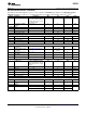
external source is shown in Typical Performance Characteristics (I
CC
vs. V
CC
).
If a fault condition occurs such that the external supply to V
CC
fails, external current draw from the V
CC
pin must
be limited as to not exceed the regulator’s current limit, or the maximum power dissipation of the IC. An external
start-up or other bias rail can be used instead of the internal start-up regulator by connecting the V
CC
and the V
IN
pins together and feeding the external bias voltage (10-15V) into that node.
A thermal shutdown protection will activate if the die temperature exceeds 165ºC, disabling the outputs (OUT1
and OUT2), and shutting down the V
CC
regulator. When the die temperature has reduced below 150°C (typical
hysteresis = 15°C) the V
CC
regulator is enabled and a softstart sequence will initiate.
Reference (Pin 2)
The Ref pin provides a reference voltage of 2.5V, ±2.4%. The pin is internally connected to an NMOS FET drain
at the buffer amplifier’s output, allowing it to sink, but not source current. An external pullup resistor is required.
Current into the pin must be limited to less than 20 mA to maintain regulation. See the graph in the Typical
Performance Characteristics.
During start-up if the pullup voltage is present before the reference amplifier establishes regulation, the voltage
on pin 2 must not exceed 5.5V. If this reference is not used the Ref pin can float or be connected to ground.
PWM Comparator (Pin 3), Duty Cycle and Deadtime
The PWM comparator compares an internal ramp signal (0 - 0.65V) with the loop error voltage derived from the
Comp pin (pin 3). The Comp voltage is typically set by an external error amplifier through an optocoupler for
closed loop applications. Internally, the voltage at the Comp pin passes through two level shifting diodes, and a
gain reducing 3:1 resistor divider. The output of the PWM comparator provides the pulse width information to the
output drivers (Out1 and Out2). This comparator is optimized for speed in order to achieve minimum discernable
duty cycles. The output duty cycle is 0% for V
COMP
< 1.5V, and maximum for V
COMP
> 3.5V. See the Typical
Performance Characteristics. The maximum duty cycle for each output is limited to less than 50% due to the
forced deadtime. The typical deadtime between the falling edge of one gate driver output and the rising edge of
the other gate driver output is 135 ns, and does not vary with frequency. The maximum duty cycle for each
output can be calculated from:
8 Submit Documentation Feedback Copyright © 2004–2013, Texas Instruments Incorporated
Product Folder Links: LM5033